Taking apart old stuff and re-using the parts to make something new is how many hackers first got started in the world of mechanical and electronic engineering. But even after years working in industry we still get that tinge of excitement whenever someone offers us an old device “for parts”, and immediately begin to imagine the things we could build with the components inside.
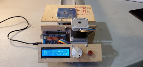
 So when [Victor Frost] was offered an old Cricut cutting plotter, he realized he could use its parts to create the camera slider he’d been planning to build. The plotter’s X stage, controlled by a stepper motor, was ideal for moving a camera platform back and forth. [Victor] wanted to build the entire thing in a “freehand” way, without making a detailed design or purchasing any new parts. So he dived into his parts bin and dug up an Arduino, a 16×2 LCD, some wires and buttons, and a few pieces of MDF.
The camera mount is simply a piece of steel that a GoPro’s magnetic mount can latch onto, but [Victor] keeps open the possibility of mounting a proper tripod ball head. The Arduino drives the stepper motor through an Adafruit Motor Shield, with a simple user interface running on the LCD. The user can set the desired end points and speed, and then run the camera back and forth as often as needed. In this way, the software follows the same “keep it simple” philosophy as the hardware design.
If you’re planning to build your own camera slider, [Victor]’s design should be easy to copy, if you happen to have an old cutting plotter. If not, you can try this simple yet well-engineered model. Want even more? Then check out this fancy multi-axis camera motion control rig.
Continue reading “Turning Old Plotter Parts Into A Smooth Camera Slider”
 While similar to the use of copper tape laid out by hand, as


