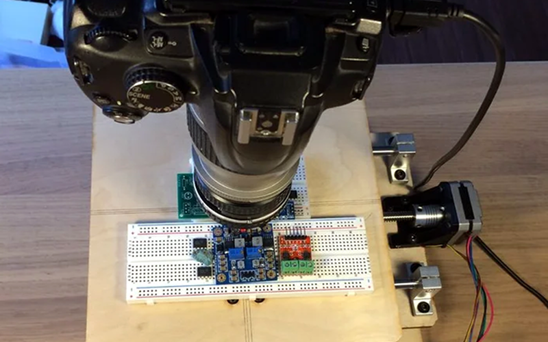
[JBumstead] didn’t want an ordinary microscope. He wanted one that would show the big picture, and not just in a euphemistic sense, either. The problem though is one of resolution. The higher the resolution in an image — typically — the narrower the field of view given the same optics, which makes sense, right? The more you zoom in, the less area you can see. His solution was to create a microscope using a conventional camera and building a motion stage that would capture multiple high-resolution photographs. Then the multiple photos are stitched together into a single image. This allows his microscope to take a picture of a 90x60mm area with a resolution of about 15 μm. In theory, the resolution might be as good as 2 μm, but it is hard to measure the resolution accurately at that scale.
As an Arduino project, this isn’t that difficult. It’s akin to a plotter or an XY table for a 3D printer — just some stepper motors and linear motion hardware. However, the base needs to be very stable. We learned a lot about the optics side, though.
Two Nikon lenses and an aperture stop made from black posterboard formed a credible 3X magnification element. We also learned about numerical aperture and its relationship to depth of field.
One place the project could improve is in the software department. Once you’ve taken a slew of images, they need to blend together. It can be done manually, of course, but that’s no fun. There’s also a MATLAB script that attempts to automatically stitch the images together, blending the edges together. According to the author, the code needs some work to be totally reliable. There are also off-the-shelf stitching solutions, which might work better.
We’ve seen similar setups for imaging different things. We’ve even seen it applied to a vintage microscope.


I think you might be off by few orders of magnitude when describing the resolution.
I agree.
Not sure about a “few orders of magnitude”… Taking that as 3 (i.e. 1000 times), you’re saying 15 mm (or 2 mm theoretical) which is clearly wrong. Even two orders of magnitude seems pretty high – that’s 1.5 mm (0.2 mm), which is probably similar to, or possibly even lower than, the heading image at the top of this article. One order of magnitude might be reasonable, but even that is dubious, especially at the lower end of things.
45,000×30,000 = 1.3 gigapixels, sounds about right to me given that it has been described as a “gigapixel microscope”.
why ?
I’ve not looked at the setup used above (yet, just about to), so I’ve no idea, but I am interested to understand your reasoning why it is off by a few order of magnitude ?
Like it is not that, that resolution is totally impossible with visible light ( e.g. https://www.microscopyu.com/microscopy-basics/resolution )
After reading all the information provided, I think that you may be wrong.
I see no reason why the images could not have a pixel resolution of somewhere between 2µm by 16µm (0.002 mm to 0.016 mm)
Maybe if an image of a diffraction grating was used with say 100 lines/mm or 300 lines/mm or 600 lines/mm which would a line spacing of 0.01 mm or 0.00333 mm or 0.00167 mm respectively (10µm,3.33µm,1.67µm). It may help give a clearer indication of the maximum resolution.
Harks back to Abbe and how he demonstrated what resolution microscopes can achieve. As an aside he clearly demonstrated how they work and why their resolution is limited by the numerical aperture. As to measuring resolution at these levels, its not that difficult. Either find small features and do some Full Width Half Maximum measurements (FWHM) or more correctly take a couple of images and do a Fourier Ring Correlation measurement (Journal of Structural Biology
Volume 183, Issue 3, September 2013, Pages 363-367).
Cough – Microsoft ICE – /cough
https://www.microsoft.com/en-us/research/product/computational-photography-applications/image-composite-editor/
Hugin
Absolutely. PTGui is good too, but it’s hard beat free.
Lots of tools for Windows/OSX/Linux, click on software at https://wiki.panotools.org/
ICE often dosnt cut it for microscope pictures it gets confused easily if you have self repeating pattern and the result is…ahem *modern art* and since you cant intervene in any way its not the right tool for the job. same goes for other free programs and even photoshop. hugin is nice and free but they still lag behind PTGui in my opinion. both have nearly identical functionality and a very nice editor but the devil is in the detail and i really believe PTGui has the better algorithmes for detection and correction.
Telecentric optics (like lenses used for machine vision), don’t distort scale at the edges so are perfect for stitching. There’s a ton about this in the forums on http://www.photomacrography.net, which is a great resource for any kind of microphotography.
I wish telecentric lenses would be more common / cheaper. They’d be great for many uses but at 200+ EUR I’ll settle for parallax artifacts.
You can make most any lens telecentric by placing an external aperture at the focal plane of the lens. Check for telecentricity by running a stack through Zerene, look at the log data and see what kind of scale factor was applied. You’re telecentric when the program doesn’t have to scale the images to properly align them.
I got a low priority project that just needs such lens at a affordable price that’s compatible with a common modern camera that a mortal also can afford.
That’s a common approach also used in professional TEM/SEM tools e.g. for brain mappings.
The newer stitching algorithms also take care of some image distortions (MIAs are mostly done at “low” mags, where modern columns are far away from the optimal beam path).
For SEM there is a different approach by using a 16k ScanGen “from Canada”.
This scans one 16k X 16k frame in “low mag” but with the finest beam/resolution.
Working with this images is “like google maps” (this mith be interesting, zoom in :) ).
I’ve got a technical question that’s bothering me… would it be possible to drop “optics” altogether… like scanning only with the matrix (scanners do that?)?
Even a scanner has optics inside to focus onto the line sensor. Unless you make essentially a pinhole camera, you will always need some optics to focus the image. The disadvantage of a pinhole camera for small stuff like this is diffraction at the aperture, and a large amount of light needed to illuminate the scene.
That’s why I used quotation marks around “optics”. I’m thinking about some basic thing just to minimize light bleed between pixels (array of fibers probably don not fall in this category). Right now I’m thinking more about microscopy and sticking a sensor to a glass shielded specimen with light passing through it.
doable but not practical if you do that the size of your pixel in your picture would directly correlate to the size of the pixel on the sensor. for microscopic pictures this would mean that the pixel are often bigger than many structures you might encounter in microscopic samples and therefor all you would get is a very rough image of your sample.
Yes, you can do this.
A simple approach is to use collimated light, and put the sensor “as close as you can get” to the subject. As someone else pointed out, the resolution in this case is on par with the size of the individual pixels of the sensor, and you might need some fancy math to get contrast back (some of the light scattering off of a structure tends to get deflected to adjacent pixels .. you can often reverse this to an extent using deconvolution).
An even better technique for lensless microscopy is digital holography. If you illuminate the subject using monochromatic light from a point source, you can do a much better job of deconvolving the resulting image. The ideal point source is coherent light (e.g. laser through a pinhole that is one wavelength in diameter). This forms a coherent wavefront that has is basically conical in shape .. that expanding cone gives a form of magnification. Farther away, more magnification .. but less energy per pixel .. and any imperfections in the setup get magnified too.
The light doesn’t necessarily need to be coherent .. an LED can be used as an illumination source. You lose some resolution, and some contrast, but if you aren’t imaging right at the diffraction limits, you can get spectacular results.
In theory, lensless digital holography has spectacular possibilities. It can give super-resolution in the z plane, it has “infinite” depth of field ..d of field limits are actually dictated by coherence, illumination intensity, physical accuracy of the system, sensor size, sensor dynamic range, thermal noise and all that good stuff, but the depth of field in a good setup is spectacular nonetheless.
And no lenses, so it is cheap. The hard part is making the light source. I have made 500nm pinholes. It took a while, and I learned (the hard way) that you need to design fiducial markers so that you can find the hole later.
In any case, pinhole issues aside, you can make one of these cameras at home, and you can get sample code online if you Google “digital holography” or “digital holographic microscopy”
Ahh .. and after going off and reading a bit, I was reminded that, rather than making a pinhole, a single-mode optical fiber is a much easier way to get something akin to a coherent point-source.
AFM… atomic resolution. There is a “hackaday worthy” version build with a piezo stage made of piezo speakers. Iirc it was a “Jugend forscht” Project in Germany. Mechanical damping of the AFM Table was done with 3 party baloons..
In that other recent hackaday article of a 75k RED camera being wrecked, I posted a link to a youtube vid from MikesElectricstuff, about a camera from a 2nd hand DNA scanner. It uses a bundled fiblre optic channel, and apparently does not use a lens in it’s intended application. In another of his video’s he spends more time on the fibre array of that (pretty weird) camera.
“The big picture” is not a euphemism.
I don’t understand the part about “3X magnification”. Cheap digital cameras can do much better than that with strictly optical zoom. What am I missing?
What you are missing is that those cheap digital cameras don’t actually do Nx magnification, they do Nx zoom. In other words, the ratio of their longest focal length to shortest focal length is N. The magnification here means the image projected onto the camera sensor is 3x the size of the object being photographed.
You’re confusing magnification with zoom.
3x zoom = minimum focal length is 1/3 the maximum. This is common and easily achievable, and in fact that Nikon zoom on its own is pretty close to this number. It’s also honestly a mostly useless specification because it doesn’t tell you where the minimum and maximum lie. A 70-300 zoom is approximately 4x, so is a 150-600 zoom, but has twice the “reach”. Nearly any of the 70-300 and 150-600 zooms on the market will be unable to even achieve 1x magnification – their minimum focusing distance is simply too long.
3x magnification = the image on the sensor plane is 3x its size in real life. Very difficult without funky optical tricks – I’ve done the reversed lens thing before, but never got good results. The aperture stop BETWEEN the lenses is a great idea I need to try.
Anyone else reminded of how CPUs (and other complex integrated circuits) are made? It used to be the case that a mask image was projected in one shot onto a wafer to react with photosensitive chemicals for processing the layers of the IC. As the scale of ICs grew, projecting in one shot became impractical, so “steppers” were used to scan the mask image out over the wafer using multiple exposures. I wonder how many “shots” are required these days for a single mask?
You can easily build a Raspberry camera microscope with resolutions down to 0.12µm/pixel, with proof that resolution really is achieved. 5$/25$ for v1/v2 camera, 5$ for Pi Zero, 15$ for microscope holder, few $s for extension rings, aluminum tubes, …:
https://www.raspberrypi.org/forums/viewtopic.php?f=43&t=210605&sid=d1ae112d8fa1f7d5a840bcf499c81033&start=50#p1409956
Forgot to mention that I recorded air bubbles moving really slowly in spittle, at 0.347µm/s speed movement in the posting preceding the pointed to.