We will admit it: mostly when we see a homebrew CPU design on an FPGA, it is a simple design that wouldn’t raise any eyebrows in the 1970s or 1980s. Not so with [Henry Wong’s] design, though. His x86-like design does superscalar out-of-order execution, just like big commercial modern CPUs. Of course [Henry] designs CPU architectures for Intel, so that’s not surprising. You can see a very detailed talk on the design in the video, below. You can also read the entire thesis project.
[Henry] starts out with a description of FPGAs and soft processors. He also covers the use of multiple instruction issue to increase the virtual clock rate of a CPU. In other words, if a 100 MHz CPU can do one instruction at a time, it won’t be any faster — in theory — than a 50 MHz CPU that can do two instructions at once. Of course, trying to do two at once has some overhead, so that won’t be completely true.
Our first impression is that the x86 instruction set is relatively difficult to implement. But [Henry] makes the point that if you can provide a robust implementation — which could include emulation of some of the more difficult parts like floating point — you can run a wealth of software with no changes.
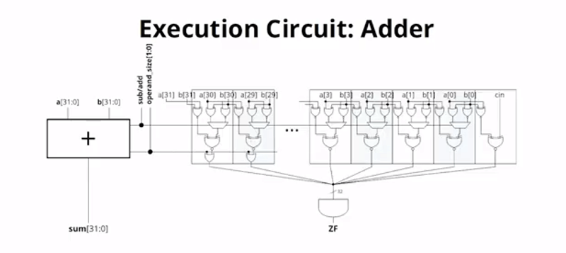
We were impressed with the method used to verify the design before it went to the FPGA using Bochs, a CPU simulator together with a known-good model of the x86. That’s especially helpful when you have to implement techniques like register renaming and a distributed matrix scheduler.
If you’ve never worked with a CPU design before, this might not be a good choice for getting your feet wet. But if you are ready to move from a toy CPU to something bigger, there’s a lot of good information in here. Need even more FPGA coaching? Try our boot camps. If you’d rather hack on RISC-V, we’ve looked at that, too.


Really x86 is a dead end architecture that’s only kept around because of large precompiled software base. My bet is that future ultra-high-performance CPUs will either run LISP ord Erlang. Sticking around with C and its abysmal multi-threading model is the reason why there’s been a stagnation in gaming since early 2010s.
According to Linus Torvalds, x86 instruction set is a good way of compressing the instruction stream of a CPU. This compression reduces the amount of memory IO to process a given task….
Maybe I misunderstand you, but CPUs dont “run” C, LISP, Erlang or whatever and never will. They only execute their instruction set (ISA). HIgh-level languages like C and LISP are compiled to this ISA (Erlang is actually using a virtual machine if I’m not mistaken). This means that CPU are already running C and LISP with no differences.
This will probably never change. You don’t build a house starting with furnitures and wallpapers. So unless there is a radical change in CPUs, like ditching the silicon transistors, CPU will run a low-level ISA.
Actually, the reverse is happening (a bit), with ARM (a RISC ISA, lower-level) crushing x86 (CISC ISA, higher-level) in power efficiency domains (mobiles…). I think there were attempts to have CPU execute JAVA bytecode, but mostly failed.
Never mind there’s no sign of it dead-ending anytime soon. Nor is gaming stagnating*.
*Maybe GPUs are “stagnating” too from that large body of “precompiled” games people keep playing.
GPU code is compiled during game loading. It is compiled from (preprocessed) shader language embedded in the game executable to native GPU instructions.
I think Tao Systems moved onto trying to do a Java bytecode processor after Taos (which was a very impressive heterogeneous multiprocessor OS) failed to go anywhere. This would be mid ’90s iirc
ISAs are a prison for performance in computing. There is a radical change coming to CPUs. Instead of “instructions” you can swap out the microcode of an algorithmic state machine to change the control plane and thus the behavior of the hardware. (see hotwright.com) You can run a program without any instructions at all. This is faster than ISA based CPUs because the hardware is built up for the application specific program. You can enjoy all the benefits of reconfigurable computing with the flexibility of an ISA based CPU.
Reconfigurable hardware has a significant performance penalty, so despite having a more optimized design is often slower.
And will be only 2x as powerful, 10000 times as large, and only the 5 richest kings of europe would be able to afford them.
Lisp does not need any special treatment from a CPU – maybe some smarter prefetch and hardware-assisted GC, not much more than that.
type tagging?
The “x86 is dead” drum has been beaten on for at least the last thirty years, and there’s still no sign of it becoming true.
There was a time that Apple insisted x86 processors were for IBM number crunching, couldn’t multitask or play games as well as a PowerPC system could.
I think we all know how that turned out.
The reason people don’t use lisp or erlang in big budget software is they don’t map well to hardware. They are “theoretical Computer Science” languages instead of practical programming languages.
Definitely alot more awesome than my SAP1 implementation. https://github.com/ellisgl/sap-1-v2-mojo
Is there an ISA with a fixed length opcode with all arguments included ?
I’m going to guess that the belt in the Mill architecture is of foxed length.
fixed, stupid typo.
ARM/ARM64 and PPC are fixed length (32-bits, or 16-bit for ARM in thumb mode), no additional bytes for operands. x86 is actually an exception with its variable length encoding (even its not the only one).
Most classic RISC architectures use fixed-length instructions (eg. MIPS, Alpha, Power, ARM, RISC-V) since this simplified the instruction fetcher and decoders. Most that survived developed variable-length versions (eg. Thumb-2, microMIPS32/64, Power VLE, RISC-V “C” extension), though curiously ARM didn’t develop a variable-length encoding for their 64-bit ISA.
Flash space (on the low end) and code cache (on the higher end) are considered more expensive nowadays than the extra transistors required by variable-length instruction encoding. It should be noted that most still only use a combination of 16- and 32-bit instruction sizes. Shortly before they died, MIPS released the nanoMIPS specification, where instructions could be 16, 32, or 48 bits long, which brought it closer to something like ColdFire, but still nothing like x86 or VAX.
VLIW architectures (eg. IA64, some DSPs) also use fixed-length encoding, though at least in the case of IA64 it kind of flips the issue on its head, by containing a variable number of instructions per 128-bit instruction word, or “bundle”.
On the Mill, every instruction/execution slot has a fixed-length binary encoding unique to the slot and flavor of mill. However most no-ops are elided making for a variable length instruction. There are also a couple places where constants and the like can be hidden in the code.
> Is there an ISA with a fixed length opcode with all arguments included ?
P8X32A and siblings.
What good of use of FPGA for running CPU in it, if you can get a twice faster ARM chip for a twice lower price?
Not everyone has a chip fab in their basement.
There are hybrid chips with ARM cores and FPGA fabric combined on one chip (Xilinx ZINQ or Altera (Intel) Cyclone V SE to name two). The ARM cores run far faster than any FPGA implementation (1GHz plus) while allowing close coupling with the FPGA Logic. The problem is that not all FPGAs come with them, and there are often parts to a task that are far easier to implement in software on a soft core than in pure logic.
Still not too close a coupling. You’ll spend dozens to hundreds of clock cycles to pass a single message between your hard CPU and an FPGA. You still may need a soft core on the FPGA side to drive all that hardware and communicate with a faster CPU with a higher latence where needed.
… Kindof. It depends on which clock cycles you’re talking about. Yes, it’ll probably take dozens to hundreds of *CPU clock cycles* in an FPGA SoC to pass from processor to fabric, but that’s because the processor runs at ~1 GHz. Fabric typically can’t run much faster than 250 MHz or so easily, and it definitely does not take hundreds of 250 MHz clock cycles. And a softcore processor in fabric isn’t really going to beat that, because it’s never going to run past 250 MHz anyway.
To me the main benefit of putting softcore CPUs in an FPGA is that you can have *lots* of them. The hard CPU is nice, but there’s still only one of them, and trying to get it to handle a bunch of realtime stuff in parallel is hard. But throwing tiny CPUs onto the FPGA and having each of them handle different tasks – that’s easy.
That’s why I tend to use the smallest softcore CPUs possible, and just dedicate each one to doing a simple thing. In a network configuration, for instance, have one handle the ARP/IP stuff and pass user IP packets forward, and then have another handle UDP packets, splitting them out by ports, and then for each UDP port have a dedicated softcore CPU handle the incoming/outgoing data stream on each one.
I’m actually talking about the FPGA-side clock. Those hundreds include data transfer, as well as request/ack latency. E.g., you have, say, a 64-bit wide Avalon slave 4kb block ram on an FPGA, driven by the hard processor. How many clock cycles would you need to fill it up, and then trigger whatever soft IP core is going to process this data on an FPGA?
I agree though that the soft cores for driving hardware-accelerated logic must be as simple as possible. There are some legitimate use cases for very wide superscalar cores, but I cannot see any reason to implement any OoO logic for them. I’m also not sure you need a lot of soft cores – one simple core driving a lot of hardware-accelerated logic is also a possibility – you can take a look at my project that I mentioned elsewhere in this thread for example.
One important use case for softcores is a simple core with some very specific hardware extensions. In this case the baseline performance of a softcore does not really matter, it only drives highly efficient hardware accelerated stuff. See an example here: https://github.com/combinatorylogic/soc
Developing on an FPGA is similar to building on a breadboard.
It is a good place to design proofs of concepts, trail the design for basic errors in its logic, etc.
Though, it isn’t impossible for an individual to go to an ASIC design company, hand over the code for the FPGA, and have them tape it out, contact a manufacturing fab, and have the design produced as an actual chip. Though usually at a fairly steep cost…
How steep? 1000’s, 10k’s, or 100k’s?
I think there’s a market for (very serious) hobbyists at the 1000’s point, and for small business/startups at the 10k’s point.
How expensive depends on your order size. The initial setup is very expensive. With current production techniques it’s really not feasible to run one-off designs, and the money isn’t there to incentivize development of new technologies conducive to small batches.
Chip fabs are EXTREMELY expensive to build.
Many logic blocks you use on an FPGA or ASIC can benefit from a small CPU to control them. This is usually much smaller than equivalent hard logic (Think of a large FSM that changes state quite slowly). In these applications performance usually is not very critical. I guess a big x86 superscalar CPU like in this article may be less useful in most FPGA designs, but it could be a way to prototype it for ASIC production.
Well in the case of the Amiga Vampire FPGA boards, the on-board soft-CPU (“Apollo”) has to be compatible with the 68000 series. Indeed the CPU core they have implemented is also superscalar, and has some additional features over the 68040/68060 CPUs for multimedia.