In the very early days of the PC revolution the only way to have a computer was to build one, sometimes from a kit but often from scratch. For the young, impoverished hobbyist, leafing through the pages of Popular Electronics was difficult, knowing that the revolution was passing you by. And just like that, the days of homebrewing drew to a close, forced into irrelevance by commodity beige boxes. Computing for normies had arrived.
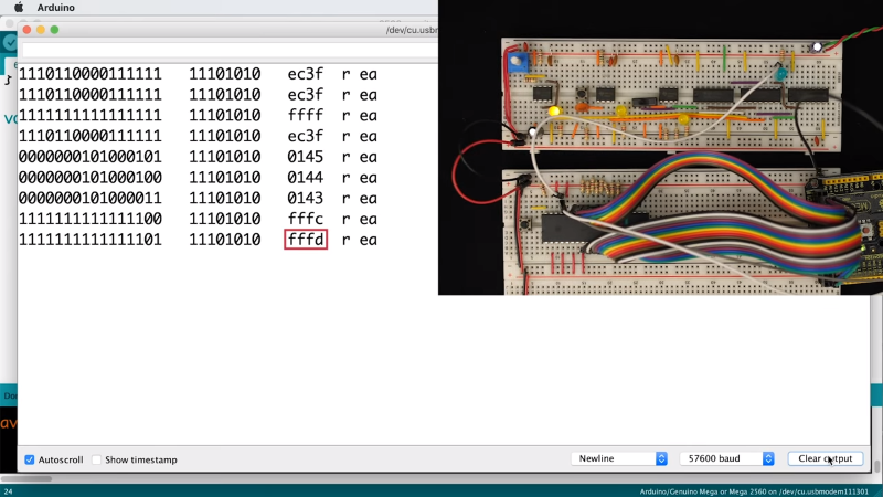
Many of the homebrewers-that-never-were are now looking back at this time with the powerful combination of nostalgia and disposable income, and projects such as [Ben Eater]’s scratch-built 6502 computer are set to scratch the old itch. The video below introduces not only the how-to part of building a computer from scratch, but the whys and wherefores as well. Instead of just showing us how to wire up a microprocessor and its supporting chips, [Ben] starts with the two most basic things: a 6502 and its datasheet. He shows what pins do what, which ones to make high, and which ones get forced low. Clocked with a custom 555 circuit that lets him single-step and monitored with an Arduino Mega-based logic analyzer, we get a complete look at the fetch and execute cycle of a simple, hard-wired program at the pin level.
This is one of those rare videos that was over too soon and left us looking for more. [Ben] promises a follow-up to add a ROM chip and a more complex program, and we can’t wait to see that. He’s selling kits so you can build along if you don’t already have the parts. There seems to be a lot of interest in 6502 builds lately, some more practical than others. Seems like a good time to hop on the bandwagon.
[Philippe] sent in this tip, which cost me $85. Thanks, [Philippe].


Ben ROCKS.
Ben absolutely rocks.
Yes he does. Also RIP Chuck Peddle who died a few days ago…The mainstream tech industry seems to have forgotten about him…..
I have about a dozen of a Motorola 146805 variant. I keep thinking I want to build something with them, someday…
I spent a couple of years of my career on those things….
So….
Are you trying to dissuade me,
or offering to help?
B^)
I actually built a Z-80 using a wire-wrap board and sockets. But I wasn’t really impressed until the Z-8 chip came out, and the number of support chips was greatly reduced. The name changed from Microprocessor to Microcontroller. Not only that, the 25 pounds of transformer and capacitors were no longer needed. The Z-8 Basic was a 44-pin board that powered many of my projects. That lasted until the popular PIC chips came along.
Got a photo?
25 pounds and capacitors? You did it wrong. My Z-80 machine, which included 6 kB of SRAM and a video timing chain, used all of 1 Amp @ 5 V. A wall wart from something else and a 7805 took care of everything.
I used a Godbout S-100 wire-wrap board and a Godbout motherboard. This was an S-100 clone, so they had big linear power supplies capable of many amps. Think 17 boards pulling 1 amp each. 20 amps with small ripple. The capacitors looked like coke cans.
http://www.s100computers.com
So therefore you associate the Z-80 with big, heavy power supplies. Got it.
Is English not your first language Jimmy?
Yes, English IS my first language, and I’m pretty good with it, if I do say so myself. I was just repeating what I got from your comment, to ensure I got it right. It’s called “reflexive listening”, and is recommended by experts for effective communications. You had stated that you were not impressed with the Z-80, and indicated that this was at least in part because of the heavy power supply, and I gave a counter-example that used no more power than a typical 6502 system. You clarified, indicating that the heavy power supply was because it was in an S-100 system. Which I took as a poor reason to be “unimpressed” by the Z-80, so I was just checking to be sure that was what you meant. No need to get personal, dickhead.
What I meant, was that the early CPU’s needed multiple support chips, while the Z-8 had the support chips built-in. In the early days, these support chips were placed on separate boards. S-100 for example. So the gist of my reply was the early CPU’s required way too many support chips. The power supply was just an exaggeration of the solutions back in the day.
Okay, thank you, that’s what I was asking. Just the same, you’re wrong in this particular case – the Z-80 didn’t require any special support chips. Lots of designers used Zilog’s SIO and PIO chips because these were what Zilog pushed in its application notes, but these were bulky 40-pin DIPs and not at all necessary; all pins except for the clock input were TTL levels (and clock in just required a pull-up resistor to make it compatible) and all of the bus connections could be made with standard 74LS chips like the 74LS244 and ‘245, in 28-pin “skinnyDIPs”. Also, unlike the 8080A, which required demultiplexing the address and data pins, these were separate on the Z-80. As I said, I implemented a complete Z-80 system that run on less than 1 Amp of Vcc, and no special chips at all. The fact that you chose a Z-80 implementation that used a bus designed for older chips like the Intel 8080A, does not reflect on the Z-80 itself.
this has been on my todo list.
Sadly, it’s on my did list back when that list was on tractor feed paper. Gotta be honest, don’t miss assembler even one tiny bit. Gonna go yell at clouds now, also, there are probably kids on my lawn.
I love this teaching style of building things bit by bit with the literal bare minimum to function.
So many others would have attached the memory or other components right way, rather then letting you see sending an instruction and reading the output right at the pin level. It always makes so much more sense to me this way.
What fun! Suggestion. Use UM61512AK-15 static RAM (64K Bytes) and decode RAM and EPROM to give 48K RAM and 16K EPROM. Or 56K/8K – easy to jumper. The RAMs are a couple bucks and are regular DIP. I ordered 4 of them – I thought – and got 16 to max out some AIM-65’s and Ohio Scientific Challenger II. I might need a GAL for decode because I have a hack in mind for 65C02 that will be beyond Ananda.
BTW, put FIG-Forth on it for the ultimate. 6502 was the first implementation and includes a brilliant inline assembler by Bill Ragsdale. 16MHz eh? Too bad Apple II depends on refresh timing for dynamic RAM in order to get video in a kind of DMA scheme.
Getting the DRAM timing right was the biggest challenge for the early home computer designers. Most, including the TRS-80 Model 1 and the Apple ][, got their DRAM refresh by mapping the display memory in DRAM, and ensuring that in the process of updating the display, each row of the DRAM was accessed within the number of milliseconds that the DRAM required. And as you say, they did this using an interleaving trick, where the video refresh was done in the clock cycles during which the CPU didn’t access the memory bus. The same could be done with higher clock speeds, but you’d basically have to slow the video counters down to still have them refresh about once every 17 ms for 60 Hz monitors. But of course you’d have to redesign the whole interleaved memory multiplexing circuit for that.
I wasn’t that brave with my first microcomputer, because I didn’t have the test equipment to help me troubleshoot if I didn’t get the timing right, so instead of DRAM, I used SRAM, which at the time limited the memory size, mainly for cost and board space reasons. The main advantage of SRAM had nothing to do with refresh, but with the fact that SRAMS had each address line pinned out separately, where DRAMS needed to be given two addresses, row and column, sequentially, which was a major PITA for someone without access to a logic analyzer.
If I remember correctly, my first homemade computer had 2 kB of display RAM and 4 kB of program, using a total of 48 Intel 2102 1Kx1 chips. But then again, programming strictly in machine code, I never ran out of program memory! By the time I built my second machine, 32 kB SRAMs were available and affordable, so even then I never had to deal with DRAM. You may notice that Ben Eater doesn’t mess with DRAM, either – these days you can’t get the old-style row-and-column DRAM chips anyway, and modern SDRAM chips are even more complicated to access..
Yeah, the AIM-65 had 2102’s with up to 4K on the4 board. There were expansion boards up to 24K on the PCB headers. Forth in ROM (Or BASIC or PLM and an assembler). The Forth manual taught everything about hardware and software. Ohio Scientific on the other hand had basically nothing but a couple docs that were a few pages. Challenger 2 – 8P DF was huge and I think 2MHz. I found a photo of one. Two units. CPU and 8″ floppy’s. I’ll have to take some good shots of mine. I can’t find anything better than this in a search. http://www.technology.niagarac.on.ca/people/mcsele/hobby/ohio-scientific-computers-osi-500-series-challenger-ii/
Westinghouse designed all sorts of DSP devices for military projects using 2102 Memory. Used as registers as well as main memory. This stuff was power hungry in the day. You needed to think about cooling. In some cases they used “cold plate” technology. The chips were thermal sealed to a stainless steel plate that had fluorocarbon running through it, as the old B-57G bombers (for example) operated at low level in the tropics.
You realized that DRAM is refreshed when you fetch a block of video data sequentially. The sense amp reads off the DRAM cell capacitor and regenerate the cell at each read cycle. Since the video RAM is in a contiguous block and if you deign the address correctly, it would go through all the rows. There is no need to have separate refresh cycles.
Understood. That’s what I meant by ensuring that each row was addressed in the process of updating the display. But you still had to generate CAS and RAS, and run the address lines through a multiplexer to feed the DRAM address lines.
I don’t know how helpful this would be for builders, but Mouser has lots of different through-hole SRAM options.
Dumb question, could he have the Arduino generate the clock for the 6502 rather than require a 555?
Yes.
I think he used the 555 mostly because he had it from a previous project: https://eater.net/8bit/clock
He also uses that board for single stepping the processor. While that would be possible to do with the arduino of course, it would require some additional code and pins.
For that matter, I’m thinking an Arduino could emulate the RAM/ROM for the 6502. I may just have to get me a DIP chip and breadboard some Arduinos to see if I could get it to work.
Just depends how much of a purist you want to be, I suppose. Judging by the kit version of this project, this will be fully independent of the Arduino, with buttons and it’s own display, once it’s complete. He’s just using it here for debugging and demonstration purposes.
You would probably want the Mega32 series instead of the usual Mega328. By the time you map out the serial port and oscillator, your ports are no longer a continuous 8-bit ports. This leads to a lot of bit operation overhead (like the digitalwrite() in Ardunio) to map bits making it very slow.
The Mega32 on the other hand have more sensible alternate function and more I/O.
its something I am very interested in .. but not that interested in when I can build an working CPM computer with about 25$ worth of parts including postage and tax
http://searle.hostei.com/grant/cpm/index.html
and have nearly a decade of ready to go working commercial software + the bare metal to fuss with
though the information is good here
ps I did build it on a perf board and its pretty bad ass
Looking at the circuit I would probably change it so that the SRAMs /WE is qualified by PHI2 rather than /CS.
This is because the address is valid sometime before PHI2 rises and /CS usually takes longer than /OE.
This would give better timing of memory accesses which would allow you to bump up the clock speed (though not a concern in this case I’d say)
The access time was a concern with EPROM back in the days. They were very slow. You are looking at 300+ns (if not 450ns) access time. Except for very early days, SRAM was faster than that.
You could get SRAM since the old 486 motherboard cache days at 15-20ns access time. Regular grades 5V SRAM were 70ns range at least 10 years ago thanks to process improvement.
Good point!, I don’t think anyone is using RAM slow enough for it to be a concern
Well, the SRAM we’re talking about here is more like 40 years ago, and there WAS no SRAM being made for 486 cache, since not even the 80286 existed yet. The SRAM you could get in the late 70s was in the 300-500 ns range as well.
Here are the timeline:
1975 – 6502 was introduced.
1975 – Intel SRAM 2114 4kb 450 ns
1976 – Intel SRAM 2115 1kb 70 ns, 2147 4 kb 55 ns – the start of faster SRAM
https://en.wikipedia.org/wiki/Random-access_memory#SRAM
I would think that by the time 6502 was generally available, there could have been fast enough SRAM.
Also we are talking about 62256 in the article. Pretty sure that they are after 1984.
So would that be from PHI2out from the W65C02?
If you’re using a WDC 65C02 it is recommended not to use PHI2O as it is no longer tested by WDC, they recommend driving everything directly from the clock source. I actually had a bunch of issues with my system that were solved by connecting the devices directly to the oscillator
As always, Ben Eater brings us an 8 bit win. His video is great for new and experienced alike!.
I had a somewhat similar plan to run a 6502 with an Arduino Mega but with simpler, if less flexible, hardware.
My plan was (is) to use an unpopulated Arduino Mega ‘shield’ put the 6502 in a ZIF socket on the board and (hard-) wire pins as required. All the signals including crystal are simulated by the Arduino and there may be simple output like LEDs to show it’s working. The program fetches and RAM are from/to Arduino RAM.
I’ve had the 6502 chip since they were old-ish tech (not vintage!) but some months ago got the ZIF socket and blank shield, but hadn’t decided how to do the witring to make the Arduino software as simple as possible.
I actually ordered this kit a few days ago along with some other parts.
Using this as a bit of a base to start from.
Some main differences in mine will be two 65c22’s for more peripherals, using 74LS138’s for address decoding, and a 65c51 for serial communication.
Will have keyboard input, serial terminal, SD card reader for mass storage, and color vga graphics (for now probably just use a mod-vga for convenience). I also want sound but haven’t decided what chips to sue for that. Possibly another 65c22 to use for an expansion port.