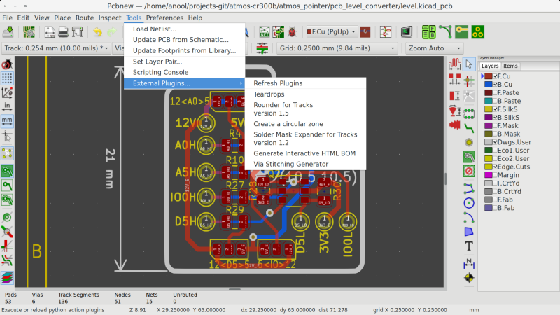
The last two years has been a particularly exciting time for KiCad, for users, casual contributors, and for the core developers too. Even so, there are many cool new features that are still in process. One bottleneck with open-source development of complex tools like KiCad is the limited amount of time that developers can devote for the project. Action plugins stand to both reduce developer load and increase the pace of development by making it easier to add your own functionality to the already extensible tool.
Sometime around version 4.0.7 (correct us if we’re wrong), it was decided to introduce “action plugins” for KiCad, with the intention that the larger community of contributors can add features that were not on the immediate road map or the core developers were not working on. The plugin system is a framework for extending the capabilities of KiCad using shared libraries. If you’re interested in creating action plugins, check out documentation at KiCad Plugin System and Python Plugin Development for Pcbnew. Then head over to this forum post for a roundup of Tutorials on python scripting in pcbnew, and figure out how to Register a python plugin inside pcbnew Tools menu.
Since version 5.0, we’ve seen an explosion of extremely useful action plugins for KiCad that have added some very useful bells and whistles. The KiCad website lists a couple of external tools, but there’s a lot of action happening out there, so we decided to round up some of the more useful ones.
KiCad StepUp Tools
Action Plugins came about as a result of work done earlier to improve the KiCad 3D model viewer by adding support for other CAD formats besides VRML. This resulted in the ability to use STEP formats for component models in KiCad 3D viewer, and the STEP export feature for the complete board. If you need nice looking renders, VRML format suits well. But if you want to import to CAD, then STEP format works better. Based on this, one early feature add-on wasn’t really an action plugin, but a workbench for FreeCAD which created a bridge between KiCad and FreeCAD. [Maurice]’s StepUp Tools offers integration between EDA KiCad and Mech FreeCAD. There’s an active thread discussing KiCad StepUp Tools on the forum with lots of demo videos and helpful assistance.
RF Tools for KiCad
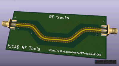 Recently, [Maurice] has released RF Tools for KiCad which include a collection of plugin’s that address a long felt need for RF design. The suite includes footprint wizards for designing mitred bends, tapered track connectors, and arc tracks (radius bends) for RF layout. These tools work by creating footprints, so it isn’t perfect, but it’s a big step in the right direction.
Also included is a set of action plugins for arc track corners, track length measurement, and a mask expansion tool. The expansion tool lets you adjust mask clearances for tracks and is handy for RF layout and for high current applications where you want to layer up extra solder on top of exposed copper tracks. It may also appeal to the artistic folks who want more control over track layout and visual design. Rounded tracks will also be pretty handy when designing flex PCBs. It’s worth pointing out that the arc action plugin will create segmented arcs while the arc footprint wizard will produce a smooth arc, so both have their pros and cons. If you get stuck, there’s an active thread on the forum for help and assistance. Check out the demo video embedded below.
Via Fencing and Stitching
When you lay out antenna traces on the PCB, it helps to have ground plane vias surrounding the track. The RF Tools suite includes a “Via Fence” generator which simplifies this task. It will add a series of vias surrounding the selected track. You can set via dimensions, pitch and distance from the track. Use this thread on the forum to get unstuck if you run in to problems.
For a while, KiCad has had a nifty via-stitching option, using which you can keep dropping vias on a net or zone manually. [jsreynaud]’s Via Stitching plugin provides a controlled way of adding a grid of vias to a zone, aka copper pour. You can set via dimensions, clearances, spacing and create random or patterned fills.
Circular Zones
At the same link, you’ll find a pretty handy Circular Zone generator. It’s a bit crusty, since changing the radius involves deleting the old zone and creating a new one, but again, we are sure it will improve pretty soon. It also lets you create circular keep-out areas within zones.
Interactive HTML BoM
By far one of the most useful plugins has to be [qu1ck]’s Interactive HTML BoM generator. Not only does it show the BoM in a nice graphical format, but it is also a very handy assembly tool that highlights the location on the PCB of any part that you choose from the BoM. Once you have a part installed, you can mark it off as “placed”, making your manual assembly process that much easier to manage. If you have questions or feature requests, head over to this forum thread.
Graphical Symbol Generator
When your design uses a part which doesn’t yet have a schematic symbol, creating it from scratch is obviously pretty painful, and prone to errors. KiSymGen is a graphical symbol generator which makes this process visual and less painful.
Teardrops
In the early days, PCB fabs often had yield issues due to offset drill holes, particularly on vias and micro-vias. One trick that PCB designers used to mitigate this problem was to use “teardrops”. The area around the pad or via that connected to the track was made into a teardrop shape, ostensibly in the hope that it would improve matters. Fabs nowadays do a pretty good job due to improved processes and accurate machines, so the jury is still out on the use of teardrops, but KiCad does have a Teardrop plugin, in case anyone wants to use it. Combined with smooth, rounded tracks, we’re guessing teardrops would be pretty helpful in the artistic PCBs department.
Spiral Coil/Inductor Generator
If you want to do something like [Carl Bujega]’s work on Designing Tiny Motors Right Into The Robot’s Circuit Board, you know you’re going to have to layout inductor coils directly on the board. SpiKi, a spiral inductor footprint generator for KiCad is what the Doctor prescribed.
This isn’t a comprehensive list by any means, so if you’re looking for a plugin we haven’t covered, then check out this roundup of plugins on the KiCad forum thread or this curated list on the xesscorp repository. If you come across one that isn’t listed, do let us know in the comments below.


So cool! We use InteractiveHTMLBOM for ZeroPhone, here’s an example: http://assembly.zerophone.org/delta-b/front_pcb/ (it’s been compiled long ago, so there might be much more features than in the version we’ve available). I also want to make a small single-button plugin that makes all the references on the board invisible – I don’t put any of the U1/R5/C14 names on my silkscreen, so I need to make them invisible one-by-one, a one-click plugin would help avoid clicking on each and every reference.
“I don’t put any of the U1/R5/C14 names on my silkscreen”
^ Why not?
I pick&place most of my component-heavy boards anyway (at our hackerspace), and I’d rather spend what little silkscreen space I have on something useful instead – obligatory “{board name} {version}, by {author}”, pinouts, usage instructions if space allows. There’s hardly ever a reason when I need to refer to a component using its reference, that usually means I have a schematic handy, and at that point, why not open a KiCad board file, too? Besides, you’ll find that Adafruit/Sparkfun do pretty much the same thing.
What usecase for references are you thinking of?
I wasn’t thinking of anything specific, just curious of your thoughts on eschewing a common practice. Thanks for the explanation! I can’t say I’ve ever really used component references either.
Part reference names are essential when debugging problems on a board with an oscilloscope. I look at the schematic to say, see the bias voltage at the base of a certain transistor. The schematic says it is Q4. Then I look at the PCB, find Q4, and now I know which transistor to probe.
Makes it more fun to troubleshoot.
Damn, gotta go tell Arduino, Raspberry Pi, Adafruit and Sparkfun engineers that it’s not possible to open a PCB viewer while you’re doing bringup/troubleshooting and they should go back to putting references everywhere. Also, it’s not possible to understand your circuit well enough to actually understand/remember which component is for what while looking at it. My take – if you’re releasing boards that will be fixed by someone who only has the schematic, by all means, put all the references everywhere. Or, y’know, release a boardview file to go with the schematic.
I design boards that are as small as possible, since I order them in 10×10 panels. Since I order them in panels and they’re just asking to be pick&placed all together, I pick&place them all in one go in our hackerspace. As a result, I don’t do all that much assembly with a soldering iron; what little silkscreen space I have is better spent on something actually useful – obligatory “board name – revision – by author” name, pinouts and usage instructions, or perhaps a “PU” (pullup) marking next to the component instead of just “R1”, or even a “R”/”C”/”L”/”D” letter under the component to help with manual assembly, should it be required. For me, the references are hardly ever useful, since you need to open the schematic to make sense of them anyway, might as well open the board file too.
Here are two panels that I’m preparing at this very moment:
1, will be pick&placed:
https://cdn.hackaday.io/images//2836921574198266677.png
https://cdn.hackaday.io/images//9636911574198277186.png
2, won’t be pick&placed:
https://cdn.hackaday.io/images//2636151574201747367.png
https://cdn.hackaday.io/images//7991061574201757789.png
All of these boards (except third-party) are available on github.com/CRImier/MyKiCad . I just love KiCad and how well it works with git =)
What’s the usecase that you’re thinking of?
I never use silkscreen (just removing solderstop on ground planes instead – much higher resolution) when using cheap boardhouses as they tend to have bad quality silkscreen and they usually print the order number on it (pcbway at least)
that can lead to confusion for them packing your order though when ordering several pcbs that look similat though
import pcbnew
class MakeRefsInvisible(pcbnew.ActionPlugin, object):
def defaults(self):
self.name = “Make references invisible”
self.category = “Modify PCB”
self.description = “Make all footprint references invisible.”
def Run(self):
b = pcbnew.GetBoard()
for m in b.GetModules():
m.Reference().SetVisible(False)
MakeRefsInvisible().register()
Formatting got mangled, you can copy it here: https://gist.github.com/qu1ck/eb3d82b91c663542f6849718d2e1552a
Thank you very much!
No need for a plugin ! You can use the Edition > “Edit text and graphic properties” tool to update all values, all references, etc
Would be wonderful if KiCad added an option for schematics-less PCB layout, where it doesn’t toss endless amounts of errors at everything one does….
Ie, just “drag and drop” footprints and traces as you desire. Maybe also add an option to specify what pins one desires to connect (as to remind oneself, a bit like a schematics, but on the fly as you go). Though, maybe also add an option to specify what things shouldn’t be connected. Just for DRC reasons.
After all, simple boards are just a waste of time to also make a schematics for. If it just contains a few buttons and LEDs, maybe a microcontroller and a few connectors, then a schematics is frankly overkill at a lot of times… Since the schematics can need just as much time to layout, as the board itself.
For more complicated designs, a schematics is though still a very useful tool. But for those PCBs that are practically describing themselves, then a schematics feels very old fashioned…
I second.
Many times i’ve need “just a pcb” with few components and i don’t want to go to the entire process of schematic, footprint selection, vias rules, etc.
Yes, there is a lot of times when one just need a board with some stuff on it.
Some people might though say, “but what if you wire something incorrectly?!”
Well, one can route a schematics incorrectly too, so there really isn’t a large difference…
And thanks to the “highlight net” tool one can rather quickly sanity check more important details of a project.
I’m new to KiCad, but can’t you do this? I just did a quick board outline plus a handful of footprints and it made gerbers just fine. Maybe I’m missing something…
I’m not new to KiCAD, and I’m surprised that you can’t do this. I’ve only done the case where you add a couple things here or there to the board, and then back-annotate to the schematic, though. Works fine.
Is it that it doesn’t want to draw a wire (e.g.) where two nets aren’t connected? I could believe that. I wonder if there’s a way to turn that checking off?
Yes, it doesn’t see a net between the pads and therefor seems to refuse connecting them.
A simple option to turn this “feature” off would be nice.
( Sorry, can’t resist )
There’s always Fritzing !
I would love to be able to draw traces from a multi-pin component back to connectors, just to make it easy to have the lines ordered in the convenient sequence on the connector. For example, and adc with 3-4 lines for spi, and not having to work out which order the pins are physically laid out while making the schematic.
I’ve run into this problem myself and didn’t discover what happened until the board came back. The footprints don’t always have pins in the same order that the schematic library has them, this SUCKS!
Tip. Attach labels to the wires in the schematic editor, then when you view the connector in PCBnew, you can see which signals go to which pins and reorder them in the schematic if necessary.
I guess you can do that if you start pcbnew standalone. just type pcbnew myboard.kicad_pcb from the command line
Check out WireIt plugin, it allows you to do exactly that.
https://github.com/xesscorp/WireIt
This plugin seems surprisingly well made.
And does just what it needs to do. (Haven’t yet tried it though, but the documentation looks very promising.)
Now if only pcbnew had this as a standard feature already….
It’s called gEDA/PCB…
I haven’t wanted anything to do with schematicless layout since I tried one time and later realized how hard that is to get right. What I really want is the easy integrated schematic+PCB experience eagle has, in a FOSS tool.
Schematics shouldn’t be a hassle. You should be able to just plop something on the schematic and click the jump to board button and it’s there, with an auto added part number and all.
In KiCad 5, this already is present, in a way – from schematic window, you only need to press F8 to update the board using the schematic data. It’s not any kind of automatic sync, but it’s literally a single-button solution and you don’t need to go through the netlist process.
StepUp tools. Sweet! That’s something I have been looking for, a way to export a 3d model of the whole board. I want to be able to 3d print a model of a board. Why? Because… reasons. This IS Hack a Day!
Anyway, I just managed to go from KiCAD to FreeCAD (which I don’t know much about.. yet). From there I bumbled through exporting to stl and Slic3r did manage to read the stl! I tried AMF too but Slic3r kept telling me the file is empty.
Anyway, the result isn’t quite printable yet, some components have parts that do not print leaving the rest floating in the air. (non manifold maybe?) Also components that live a-top leads seem unlikely to print via FDM.
I would like to make a second set of component models. I would like to make one that is less realistic looking but totally printable. Then I would like the ability to switch between the two when rendering.
Hey, it’s OSS. I should do it myself right? I’m not quite ready to take that on yet. When I am maybe I will. I hope somebody beats me to it though.
I used that quite a few times and quite a while ago, maybe >2 years already. I agree with the problems you are facing, some models make it hard to 3D print if you want to know how it all integrated. But that is just a limit of 3D printing, not Kicad. Depending on what you are trying to print, support generation in the slicer helps sometimes, like if you start with a horizontal PCB and everything is built on top of that.
That first link is a 404.
Weirdly I was playing with the plugins on the Xess corp 3rd-party-tools github just last night, and tried their updated teardrop inserter on my current project just this afternoon. Whilst the aforementioned version is gui-based and easy to add and remove teardrops, it only works on via connections, not pads and T-tracks, as advertised, which is a shame. I guess something changed in the latest KiCAD update?
Anyway, this is all good stuff, and learning the plugin interface is on my todo list (albeit a very long one) of things to study and use for future dev.
I’m finding most of my paid work now involves a fair element of PCB design, even for a first prototype, so I’m currently building a four-monitor monster of CAD setup, purely for KiCAD work. And maybe a little splash of LTspice.
See how fast KiCAD is changing! I edited this article a few days ago, and already we have linkrot.
Fixed up to the latest version of the Plugin intro. Thanks for the catch.
Two monitors (schematic and PCB) for KiCAD is pretty close to a must. I’ve done some design standalone on my laptop, and the combo of no scroll wheel and the single monitor really feels gimped. Still, I can’t think of what four monitors would get you. A third for datasheets might be nice…
Sure, two is a minimum for sanity. For the third, I’m finding for ‘innovation’ type projects, where size is everything, I’m relying heavily on the 3D view, so I like to have that open as well. The fourth screen would be for datasheets. It really is a luxury, but having the screen space means I can have another task going, like VNC to my windows box for my email and project journals, or a webcam view of the 3D printer going.
My workshop setup means that I don’t need a desk for CAD, just a comfy chair and a floor-standing monitor/keyboard stand. When doing assembly, then two monitors can rotate so I can view the layout and a visualplace session without moving from my assembly station all the time, which will save my back and my time.
I certainly find two screens limiting, and when buying a monitor mount I found a square one, with two sets of arms, so three monitors seemed a bad fit. Plus, I scrounged and fixed six identical (borked) monitors, so you know, why the heck not :)
I always thought the teardrop shape was to prevent having a sudden step in the width from the through-hole pin to a track, so that the trace was less likely to crack at the stress-riser a step produces.
That has certainly been my experience.
Any comments?
Yes, that is correct. It is especially used for flexible PCBs.
Teardrops are still very relevant for flex PCBs
Teardrops have many uses. The added width allows for greater misalignment of vias during production, it increases mechanical strength, and it adds insurance against open connections caused by accidental over-etching.
Wow, the last time I designed a board CERN were just getting involved with kicad and adding the push/pull router. The progress they have made since then is amazing!
The replicate layout plugin is a must have if you do a lot of work with (identical) hierarchical sheet; https://github.com/MitjaNemec/Kicad_action_plugins
Not a plugin, but kicad-3d-models-in-freecad is an amazing tool for creating parametric 3D models and have complete and perfectly accurate 3D models of your boards.
KiCad is progressing so fast in everything except usability. I hear they’re making progress, but it’s still nowhere near even LibrePCB, which is really just missing DRC, import from SnapEDA, and a few minor tweaks.
There’s a lot of usability progress in KiCad5, you should check it out – I got used to KiCad 4, switched to KiCad 5 now – more pleasant to use, no doubt.
Agreed, KiCad 5 is a big improvement.
I’d like to try that color scheme, I’m mostly a beginner, does anyone know where I can find that/set it up? I currently have some Dark mode theme, but I don’t even remember how I set it up.
If you double-click on a colour swatch, you can set colours and transparency.
I believe this tool deserves a mention here: https://gitlab.com/dren.dk/kicad-util
Although not an action plugin the tool is useful for panalization and designing mouse bites
And if you’re looking for a known-working tool that can do panelization from both KiCad and other software, with different boards and a relatively small amount of bugs, I have a tutorial here: https://hackaday.io/project/19202/log/59210