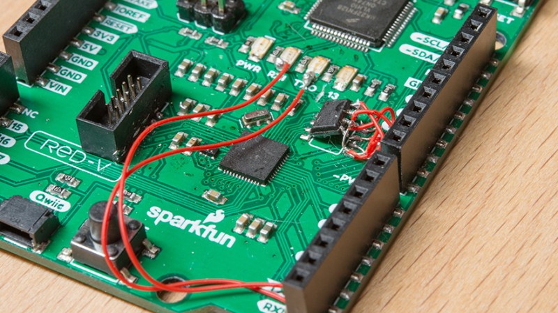
If you design printed circuit boards, then you will have also redesigned printed circuit boards. Nobody gets it right the first time, every time. Sometimes you can solder a scrap of 30gauge wire, flip a component 180°, or make a TO-92 transistor do that little pirouette thing where the legs go every-which-way. If you angered the PCB deities, you may have to access a component pad far from an edge. [Nathan Seidle], the founder of Sparkfun, finds himself in this situation, but all hope is not lost.
Our first thought is to desolder everything, then take a hot iron and tiny wires to each pad. Of course, this opens up a lot of potential for damage to the chip, cold joints, and radio interference. Accessing the pin in vivo has risks, but they are calculated. The idea is to locate the pin, then systematically drill from the backside and expose the copper. [Nate] also discovers that alcohol will make the PCB transparent so you can peer at the underside to confirm you have found your mark.
In a real, “fight fire with fire” idea, you can rework with flex PCBs or push your PCB Fu to the next level and use PCBs as your enclosure.


I’ve made mistakes before. Missing wire between 2 chip, forgot to do DRC to discover crossed trace, and once used SOIC footpad for a TSOP chip. Trying to wire up a dozen chips x 16 pins each wasn’t fun.
Those of us that started with pads and tape tend to get things right the first time.
I remember my EET241 teacher talking about the cost of producing and shipping boards for his company. Sometimes, it was cheaper for an engineer to charter a plane and fly to the fab house to get the boards in person. If I was up against that kind of barrier, I would spend more work on the first board too!
Every teacher tells those stories. It must have happened at least once in the world.
These days you can get 10 boards made for like $5 + $14 shipping and have them in 2 weeks.
Where do you get your 14-layer with 2+2 blind and buried vias for $5 each?
I can have them in my hands in four business days and that’s from China to NZ!!
Or shipped overnight for 100ish… And in a professional setting, that’s nothing compared to two weeks of lost production time.
The PCB I had in China charged $15 for DHL international service and only took takes 2 days to deliver a few years ago. Their outsourced 2 layers prototype PCB took about 5 days.
Long time ago when I actually made pcb’s that way we used to make the original at a 2:1 size and use a photocopy machine to produce the transparent films.
You can actually set the aspect ratio wrong, flip the original and do many more nice mistakes even when the design is right.
I can remember the first 3 boards I designed our teacher told us to design it on transparent paper with pens it was hell but since then I didn’t do many mistakes afterwards
Right, “you” did the TO92 pinout wrong, fun thing is when your parts house swear a transistor is an exact exact equivalent, practically a second source of the original, then you get it and it’s BEC or ECB instead of EBC
My parts warehouse was the low-ball seller on eBay. I knew the risk and it bit me. I gambled my time against saving a few cents on transistors. There were other problems with the first draft of the board that started with a shoddy Instructable. In the end, it was a cheap lesson with no professional stain on my record.
You can bend the through hole transistors to suit the footprint so it is no big deal. You could put the wire insulation to prevent pins crossing from getting shorted.
For SMT transistors, the pinout is more uniform. I haven’t done through hole parts for ages and won’t go back.
Although, you can often set a SOT23 transistor on a SOT23 footprint 120 degrees off and fix SMT transistor layout problems. Or if you pour ground planes everywhere, use 2 of the 3 pads, scrape off the soldermask, and 180 the SOT23 (only applicable if it’s switching to ground, obvs.).
This makes me wonder if PCB vendors could offer clear (or at least translucent) board material, to directly enable this sort of hacking.
Order it with no soldermask. It’s not clear, but it’s kinda translucent under bright light.
I think a pogo-pin “back-pack” could work with smaller holes and pads when soldering is not an option.
Our ATE test boards cost about $30K each, and it’s not unusual to have a layout error, and pretty common to have a design error that only becomes obvious once the new chip comes back from fab and the test engineers are having trouble with the test program they wrote. I get to mod a 30 layer board every couple of months, involving cutting an inner-layer trace. This has worked pretty well: print out the whole stackup on overhead transparency film, in black, with the offending trace in red or something. Stack it up and hold it up to the light and find a place where there aren’t any overlaying traces (ground planes kinda okay, hopefully not power and ground on adjacent layers.) Lay the transparencies on the board lined up with whatever is on the top or bottom layer. Our boards always have mounting holes so we can punch holes through the transparencies and bolt them to the board. Then put a pin or something through the transparencies where you want the hole to go and mark up the soldermask. Undo everything, and solder wires to the offending trace end points and hook a DMM to them, preferably one that beeps when it senses continuity. Then stick the whole works on your milling machine, or in a pinch your drill press. Clip (scope ground clip with a spring end) a wire onto the drill, and another onto one of the DMM traces, and hook that to a second DMM, same deal. Then you can drill in at the mark, and you’ll hear it when you hit the trace, and you’ll hear it when the trace has been cut through. On my mill at home I can consistently manage this on a board that has 4.5 mil inner layers, without hitting stuff on the next layer down. Then test to make sure you didn’t short planes you cut through. I end up having to clean up with an x-acto knife sometimes, but not often. We always have to remake the boards before release to production, but we can save months and sometimes a spin or two of the boards, with this.
Wow, thanks for these insights.
That’s gold. Thank you.
With a CNC mill you could use the auto z-probe feature to automatically stop as soon as it hits the trace.
I don’t know about current availability, but I do know that a long time ago there were “electronics training kits”, mainly intended for youngsters to use when first learning electronics. The had bags full of a wide variety of commonly used components such as resistors, capacitors, IC chips, etc. But for the design engineer, the most important was a “board” that did not require soldering (safety for use by small children). Instead, they had springs that you could attach your wires to. That way you could try out a variety of components and combinations before committing them to being soldered to an actual printed circuit board. Even before designing the layout of the actual PC board itself. Other kits used boards with small holes and connections underneath, so that you could just push the wires (and IC chip legs) into the holes to connect them. These “toys” actually can become quite useful for someone designing boards. And hey, they are also a fun way to try out new hacks.
I assume that you mean kits like this one: https://www.parts-express.com/elenco-130-in-1-electronics-playground-kit–320-064
Sparkfun used to carry the springs to make your own: https://www.sparkfun.com/products/retired/11822
They still seem to be available in Australia: https://core-electronics.com.au/spring-connectors-pack-of-10.html
I’m old enough to remember using Fahnestock clips on my childhood projects: https://en.wikipedia.org/wiki/Fahnestock_clip
GRMBH. this reminds me of the one time the datasheet of the 9dof qfn chip contained the pinout LOOKING FROM BELOW. the chip was a 3x2mm thing and i had to dead bug style solder the thing in place. Not funny.
I was hired as a lone EE in a company of MEs. They had bid on an electronic product design, that was part of a mechanical product they were also supplying (two VME backplane cards for Qualcomm, as part of a custom VME chassis design), won the bid, and then hired me to deliver. Not to denigrate MEs, but they generally don’t know beans about the intricacies of digital and analog circuit design! I had to redesign both cards to meet the customer’s requirements. My boss, the VP of Engineering grew to dislike the term “respin”, but it’s sometimes a fact-of-life. He didn’t seem to understand that some parts, listed as ‘active’ or “in production” can reach end-of-life with little or no warning, and all you can do is redesign a PCB to accommodate a new design, with new components. This happens in telecom all the time: a particular relay is here today, and gone tomorrow. The only other option is to try and throw tons of money at semiconductor mfgrs to keep a particular part in production. But you can quickly run out of money if that happens to multiple parts.
Even a part in production can become unavailable for 6 months to a year, if some other customer buys up all the supply. That happened to my son’s company once, when the accelerometer they were using got used for the first run of the MicroBit boards.
It’s a shame Sparkfun seem to still be using Eagle. They made a good effort a couple of years ago to migrate to Kicad, released a bunch of footprint files, and Nate himself (IIRC) wrote an excellent tutorial on how to use Kicad. I won’t link to it here, because it is now sadly outdated.
Can anyone from Sparkfun comment on the adoption of Kicad there?