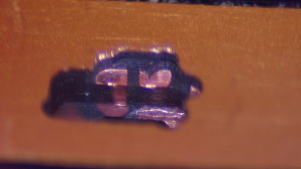
Homebrew TEM Cell Lets You EMC Test Your Own Devices

Submitting a new device for electromagnetic compatibility (EMC) testing seems a little like showing up for the final exam after skipping all the lectures. You might get lucky and pass, but it really would have been smarter to take a few of the quizzes to see how things were going during the semester. Similarly, it would be nice to know you’re not making any boneheaded mistakes early in the design process, which is what this DIY TEM cell is all about.

We really like [Petteri Aimonen]’s explanation of what a TEM cell, or transverse electromagnetic cell, is: he describes it as “an expanded coaxial cable that is wide enough to put your device inside of.” It basically a cage made of conductive material that encloses a space for the device under test, along with a stripline going down its center. The outer cage is attached to the outer braid of a coaxial cable, while the stripline is connected to the center conductor. Any electric or magnetic field generated by the device inside the cage goes down the coax into your test instrument, typically a spectrum analyzer.

[Petteri]’s homebrew TEM is made from a common enough material: copper-clad FR4. You could use double-sided material, or even sheet copper if you’re rich, but PCB stock is easy to work with and gets the job done. His design is detailed in a second post, which goes through the process of designing the size and shapes of all the parts as well as CNC milling the sheets of material. [Petteri] tried to make the joints by milling part-way through the substrate and bending the sheet into shape, but sadly, the copper didn’t want to cooperate with his PCB origami. Luckily, copper foil tape and a little solder heal all wounds. He also incorporated a line impedance stabilization network (LISN) into the build to provide a consistent 50-ohm characteristic impedance.

How does it work? Pretty well, it seems; when connected to a TinySA spectrum analyzer, [Petteri] was able to find high-frequency conductive noise coming from the flyback section of a switch-mode power supply. All it took was a ferrite bead and cap to fix it early in the prototyping phase of the project. Sounds like a win to us.

Illustrated Kristina with an IBM Model M keyboard floating between her hands.

Keebin’ With Kristina: The One With The Music Typewriter

This edition’s community build comes from the Yes They Could, But Should They Have? file. Well, I ultimately say yes, this is intriguing. Redditor [dj_edit] looked at the venerable Model M and thought, this buckling-spring masterpiece can yet be improved upon. Yeah! Well, to each their own. I must say that it does sound great, especially with the solenoid feedback enabled via rotary encoder. Just check out the typing test.

To be clear, this is essentially a new keyboard that fits inside a Model M case, but that alone is quite a feat, especially if you consider the curvature of the backplate. Because of this hurdle, [dj_edit] went with 1 mm FR4 for the switch PCB, which is a nice compromise of sturdiness and flexibility.

Underneath those stunning reproduction keycaps are Kailh box white switches, which are pretty chonky-sounding on their own. But turn on that sweet solenoid action and you really get noisy.

Those box whites are sitting in hot-swap sockets, a design decision that kind of made things difficult because of the curvature. [dj_edit] ended up using an acrylic plate that gets bent to match the curvature by the switches themselves.

Continue reading “Keebin’ With Kristina: The One With The Music Typewriter”

Shot of CubeTouch, a six sided cube built out of PCBs with each of the top PCB allowing for diffusion of the LEDs on the inside to shine through

Keyboard Shortcuts At The Touch Of A Planetary Cube

[Noteolvides] creates the CubeTouch, a cube made of six PCBs soldered together that creates a functional and interactive piece of art through its inlaid LEDs and capacitive touch sensors.

The device itself is connected through a USB-C connector that powers the device and allows it to send custom keyboard shortcuts, depending on which face is touched.

Finger touching the top of a CubeTouch device

The CubeTouch is illuminated on the inside with six WS2812 LEDs that take advantage of the diffusion properties of the underlying FR4 material to shine through the PCBs. The central microprocessor is a CH552 that has native USB support and is Arduino compatible. Each “planet” on the the five outward facing sides acts as a capacitive touch sensor that can be programmed to produce a custom key combination.

Assembling the device involves soldering the connections at two joints for each edge connecting the faces.

We’re no strangers to building enclosures from FR4, nor are we strangers to merging art and functionality. The CubeTouch offers a further exploration of these ideas in a sweet package.

The CubeTouch is Open Source Hardware Certified with all documentation, source code and other relevant digital artifacts available under a libre/free license.

Continue reading “Keyboard Shortcuts At The Touch Of A Planetary Cube”

PCB internal bodge

PCB Microsurgery Puts The Bodges Inside The Board

We all make mistakes, and there’s no shame in having to bodge a printed circuit board to fix a mistake. Most of us are content with cutting a trace or two with an Xacto or adding a bit of jumper wire to make the circuit work. Very few of us, however, will decide to literally do our bodges inside the PCB itself.

The story is that [Andrew Zonenberg] was asked to pitch in debugging some incredibly small PCBs for a prototype dev board that plugs directly into a USB jack. The six-layer boards are very dense, with a forest of blind vias. The Twitter thread details the debugging process, which ended up finding a blind via on layer two shorted to a power rail, and another via shorted to ground. It also has some beautiful shots of [Andrew]’s “mechanical tomography” method of visualizing layers by slowly grinding down the surface of the board.

[Andrew] has only tackled one of the bodges at the time of writing, but it has to be seen to be believed. It started with milling away the PCB to get access to the blind via using a ridiculously small end mill. The cavity [Andrew] milled ended up being only about 480 μm by 600 μm and only went partially through a 0.8-mm thick board, but it was enough to resolve the internal short and add an internal bodge to fix a trace that was damaged during milling. The cavity was then filled up with epoxy resin to stabilize the repair.

This kind of debugging and repair skill just boggles the mind. It reminds us a bit of these internal chip-soldering repairs, but taken to another level entirely. We can’t wait to see what the second repair looks like, and whether the prototype for this dev board can be salvaged.

Thanks to [esclear] for the heads up on this one.

RGB Glasses Built From PCBs

Shutter shades were cool once upon a time, but if you really want to stand out, it’s hard to go past aggressively bright LEDs right in the middle of your face. A great way to achieve that is by building a pair of RGB glasses, as [Arnov Sharma] did.

The design intelligently makes use of PCBs to form the entire structure of the glasses. One PCB makes up the left arm of the glasses, carrying an ESP12F microcontroller and the requisite support circuitry. It’s fitted to the front PCB through a slot, and soldered in place. The V+, GND, and DATA connections for the WS2812B LEDs also serve as the mechanical connection. The right arm of the glasses is held on in the same way, being the same as the left arm PCB but simply left unpopulated. A little glue is also used to stiffen up the connection.

It’s a tidy build, and one that can be easily controlled from a smartphone as the ESP12F runs a basic webserver which allows the color of the glasses to be changed. It’s not the first time we’ve seen a flashy pair of LED shades either! Video after the break.

Continue reading “RGB Glasses Built From PCBs”

Laser Blasts Out High-Quality PCBs

With how cheap and how fast custom PCBs have gotten, it almost doesn’t make sense to roll your own anymore, especially when you factor in the messy etching steps and the less than stellar results. That’s not the only way to create a PCB, of course, and if you happen to have access to a 20-Watt fiber laser, you can get some fantastic homemade PCBs that are hard to tell from commercial boards.

Lucikly, [Saulius Lukse] of Kurokesu fame has just such a laser on hand, and with a well-tuned toolchain and a few compromises, he’s able to turn out 0.1-mm pitch PCBs in 30 minutes. The compromises include single-sided boards and no through-holes, but that should still allow for a lot of different useful designs. The process starts with Gerbers going through FlatCAM and then getting imported into EZCAD for the laser. There’s a fair bit of manual tweaking before the laser starts burning away the copper between the traces, which took about 20 passes for 0.035-mm foil on FR4. We have to admit that watching the cutting proceed in the video below is pretty cool.

Once the traces are cut, UV-curable solder resist is applied to the whole board. After curing, the board goes back to the laser for another pass to expose the pads. A final few passes with the laser turned up to 11 cuts the finished board free. We wonder why the laser isn’t used to drill holes; we understand that vias would be hard to connect to the other side, but it seems like through-hole components could be supported. Maybe that’s where [Saulius] is headed with this eventually, since there are traces that terminate in what appears to be via pads.

Whatever the goal, these boards are really slick. We usually see lasers used to remove resist prior to traditional etching, so this is a nice change.

Continue reading “Laser Blasts Out High-Quality PCBs”

An Easier Way To Roll Your Own LED Ball

Yes, circuit sculptures are amazing. But the patience and skill required puts most of the designs we’ve seen fairly far out of reach of the average beginner. We totally understand — not everyone finds fun in fiddly, structural soldering.

[Hari Wiguna] was captivated by the LED ball that [Jiří Praus] made last Christmas and figured there had to be less painful ways to cover a sphere in blinkenlights than printing a negative to use as a soldering jig. Turns out there is at least one way — just design the structure to use PCBs in place of brass rod, and fit everything together like a 3D puzzle made of FR4.

This SMD LED ball is almost ready for prime time. [Hari] wants this to be accessible for everyone and completely parametric, so he’s still working out the kinks. Check out the current form after the break as [Hari] rolls the ball through the various display modes using an Arduino and talks about the failures along the way, like having to file out the LED slots because they were designed too tightly the first time. [Hari] is also working on the friction fit of the pieces so the ball is easier to assemble, especially at the beginning.

3D prints as circuit sculpture soldering jigs are great tools, don’t get us wrong. How else are you gonna solder brass rod together on a curve?

Continue reading “An Easier Way To Roll Your Own LED Ball”