
[Jan Mrázek]’s success with 3D printing a solder paste stencil is awfully interesting, though he makes it clear that it is only a proof of concept. There are a lot of parts to this hack, so let’s step through them one at a time.
First of all, it turns out that converting a PCB solder paste layer into a 3D model is a bit of a challenge. A tool [Jan] found online didn’t work out, so he turned to OpenSCAD and wrote a script (available on GitHub) which takes two DXF files as input: one for the board outline, and one for the hole pattern. If you’re using KiCad, he has a Python script (also on GitHub) which will export the necessary data.
The result is a 3D model that is like a solder paste mask combined with a raised border to match the board outline, so that the whole thing self-aligns by fitting on top of the PCB. A handy feature, for sure. [Jan] says the model pictured here printed in less than 10 minutes. Workflow-wise, that certainly compares favorably to waiting for a stencil to arrive in the mail. But how do the actual solder-pasting results compare?
[Jan] says that the printed stencil had a few defects but it otherwise worked fine for 0.5 mm pitch ICs and 0402 resistors, and the fact that the 3D printed stencil self-registered onto the board was a welcome feature. That being said, it took a lot of work to get such results. [Jan]’s SLA printer is an Elegoo Mars, and he wasn’t able to have it create holes for 0.2 mm x 0.5 mm pads without first modifying his printer for better X/Y accuracy.
In the end, he admits that while a functional DIY solder stencil can be 3D printed in about 10 minutes, it’s not as though professionally-made stencils that give better results are particularly expensive or hard to get. Still, it’s a neat trick that could come in handy. Also, a quick reminder that we stepped through how to make a part in OpenSCAD in the past, which should help folks new to OpenSCAD make sense of [Jan]’s script.


This has me wondering if my Eagle -> Fusion 360 would work to capture the layout and board dimensions. Need to check if my older Prusa can print to a fine-enough resolution. The idea of self-registration is especially appealing.
The stencil made in the article is from an SLA printer. My doubts about using FDM printers for this mostly come from the surface not being very smooth, which I expect to cause problems with the paste bleeding under the edges, and losing a lot of solder paste to the surface. But I’ll be happy to believe it when I see it!
Depends on what type of build-plate you use and which side the PCB sits on, if you print the stencil on glass and then put the side that was on the build-plate onto the PCB you should get a very solid seal for this application
You’d lose the registration feature that way, although my initial thought on seeing this was that 3d printing a jig to hold the board and a conventional stencil makes a lot of sense.
Actually I just recently did this and it works really well. Make sure you make the jig less thick than the pcb so the pcb sits on top. I would try 1.5mm for a 1.6mm layer board. My jig was too tall so I had to shim up the center with some painters tape. I attached the Jig using some tape as well.
using the bed side as the layer where you apply the paste would let you make the register perfectly, also giving you a smooth surface (literally glasslike if you use a glass surface)
MAYBE.. with lots of sanding.
The stencils I order are usually 0.1 or 0.12 mm thick. This applies a good amount of paste.
My first layer is usually 0.3mm thick. That’s too thick and would apply too much paste. You could reduce the size of the holes by 3x, but then the paste would stick in the stencil and not to the board.
My nozzle is 0.4mm, but I normally print at 120 or 130% on the fist layer. So 0.5mm is the smallest feature you can make.
I’d say… I’m not going to try it. Not worth my trouble.
I would think it would be worth it to get a smaller nozzle, to get both better resolution and a thinner first layer. Pretty easy adjustment, I’d say, compared with what it takes to either order a stencil or manually apply paste. I’m kind of warming up to the idea.
I don’t think you can print a “useful” stencil on an FDM printer. Maybe for a very specific case, with large pads, large (>0805) components and enough clearances between pads… I would guess that you are far quicker in making a few stencils out of a transparency film by printing on it with a 2D desktop printer and cut out all the pads with a hobby knife. Tuning an FDM (and the slicer) for reliable printing of very fine structures and thin layers with tiny nozzles is quite a pain in the butt by itself. And then you are still left with figuring out all the compensation parameters to get the right amount of paste on a pad with “thicker than normal” stencils. And on top of that, i can see that you would probably have quite a lot of problems with paste sticking in the printed stencil too good, giving you even more stuff to manually rework.
I can’t see why you wouldn’t be able to use 0.1mm first layer height and a 0.2mm nozzle (or .25) with 100% extrusion width. then if you use a glass bed, you simply put the top layer (rough side) towards the PCB, and have a nice smooth surface at the top to apply the paste.
anywyas yeah it’s a royal PITA, but don’t dismiss it so easily. pretty sure you just need some good autolevel
I’m wondering if that rubbery glue you often get on peal open spam post would be good to print an etching mask for copper clad board.
Seems like a good train of thought. But I don’t think you want to put that stuff through a 3D printer. it MIGHT work with hot glue, though this could be trouble to remove.
I’m Thinking PLA would be a mighty fine choice. Fairly chemical resistant. Easy to remove with low enough heat to avoid damaging the board. Directly printable with a bit of dialing in on, say, an Ender 3 with an ABL system.
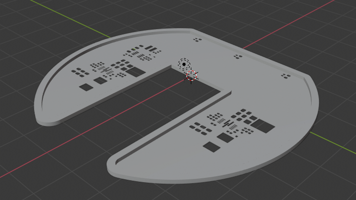
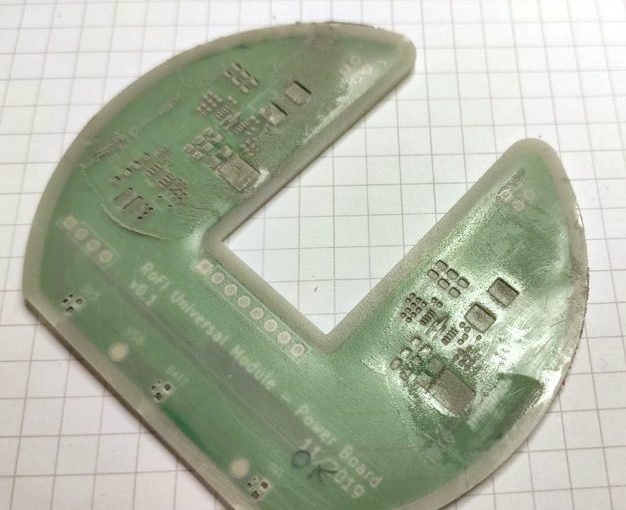
I can’t help but wonder what the PCB shown is for, clearly some pretty specialised mechanical constrains on it given the shape of the edge, what does it have to fit into? Would like to know.
Looks similar in shape to the ESC that fits inside the BLDC hub motor for an Ebike.
It is power board for RoFIbots: https://ro.fi.muni.cz/
This violates the cardinal rule of clickbait: to any question posed in a headline, the answer is NO!
Heh..makes me wonder if you could use a finely tuned printer with a smaller nozzle( say .2mm) and directly print a resist mask down for etching…hmmm…need some 235 x 235 copper clad….
This is a really neat idea! But I think it is more imaginable for SLA printer – you attach copper clad to the build platform and print a single layer. The resin sticks really well to metals.
On the other hand – if you already have a resin printer, you can directly expose photoresist using the UV light – there are already projects to do so: https://github.com/Reonarudo/pcb2photon
In theory, that could work. The issue i see is that the layer of printed plastic would be a very bad, very inconsistent etch resist mask. The edge where the plastic meets the copper is just not going to be clean and constistent enough. The acid will find a way to get into every little flaw of the etch mask, eating away copper it should not. Maybe you would get away with it on a board designed specifically for this, with huge traces and clearances. But at that point, you are technically in the realm where using perforated prototype-boards and manual wiring are just as viable (and way quicker) than trying to brute force an unreliable DIY-PCB fabrication…
“The edge where the plastic meets the copper is just not going to be clean and constistent enough.”
Don’t see why not – I get very clean edges, especially on the first layer.
“The acid will find a way to get into every little flaw of the etch mask, eating away copper it should not.”
Most every little flaw in FDM is between the filament lines. Keeping in mind that the filament is the resist, this would only mean that wide traces might have pinholes in them. Narrow traces, not an issue.
“you are technically in the realm where using perforated prototype-boards and manual wiring are just as viable (and way quicker)…”
You’re saying that hand-wiring is faster than printing a SINGLE LAYER on an FDM? You are either the fastest wire cutter and stripper on the planet, or pathetically slow in setting up FDM.
Furthermore, for those projects that would otherwise be done on perfboard, a printed circuit board offers superior properties in almost every way. If you want to trash this method, it would probably be more effective to compare it to using a CNC router, which at least puts us in the apples and apples realm.
And yeah, this brings me back to CNC routing, where you can do the copper pattern and the drilling and outline routing, all with one machine, without having to align the board between passes.
I actually tried this a long time ago, it works but there’s not much sense to it considering you can make a springy jig with a couple of LM8UU’s and two small M8 smooth rods in order to plot on the PCB with a permanent marker. then you just use FlatCAM to make the gcode. it’s a pain in the ass but once you get it correctly dialed in (and find a good brand of permanent marker) you’re good to go
That doesn’t sound much worse than pretty much ever other etch-at-home method I have ever tried!
discalimer – I have not tried UV yet
You know, if you already have an FDM printer, you’re just a couple steps away from a pen plotter. A fine-point paint pen would probably be less troublesome than FDM.
I realize this is something of an “everything is a nail” situation, but I’d rather rig up a syringe to a 3D printer, and deposit the solder paste directly.
Just saying, sometimes it may be better to use the 3D printer to make the right tool for the job…
How would you do that on MSLA printer?
Um. I wouldn’t. SLA printers aren’t nearly as hackable as FDM.
We had this machine at company I worked. The XYZ router was solid, but nothing special. But the actual soldering paste dispenser was expensive and complicated. You can’t use syringe, there was screw, which applied the paste to PCB. This is it: https://www.dimadispensing.eu/dispensing/products/valves/rotary-valve-dd-5100
Sadly, I never saw it working, asi it was already broken, whan I first use the machine. But the cleaning was nightmare, I heard.
that’s interesting, but i think i saw one with a syringe, probably in this website too. I figure you need a sufficiently fast (and torquey) extruder mechanism to be able to retract fast enough, like on a regular 3d printer (retractions upwards of 80mm/s do help).
that said, it’s almost definitely possible to reverse engineer that screw and print one out to test.
I wonder if using a glass syringe would help with retraction, I have a couple lying around, and they slide effortlessly. although flux could make that much worse
Does anyone have any brand recommendations for tacky hobbyist paste?
Tacky hobbyists have their own kind of paste?!?
If you use kicad you can use the plot function and go directly to svg; I use that approach to cut stencils from 4 mil mylar.
For a partial assembled PCB where certain components were not possible to factory assemble I designed small stencil pads in Fusion360 and printed them on my Tevo Tornado (on glass plate), one layer PLA. They work very well.
What were the settings in your Slicer program that you found most ideal for this to work well?
Nothing special, just one layer thick. I guess you have to experiment a bit to get is as thin as possible without warping on your printer.
Life saver! Great site, does the trick.