You might have caught Maya Posch’s article about the first open-source ASIC tools from Google and SkyWater Technology. It envisions increased access to make custom chips — Application Specific Integrated Circuits — designed using open-source tools, and made real through existing chip fabrication facilities. My first thought? How much does it cost to tape out? That is, how do I take the design on my screen and get actual parts in my hands? I asked Google’s Tim Ansel to explain some more about the project’s goals and how I was going to get my parts.
The goals are pretty straightforward. Tim and his collaborators would like to see hardware open up in the same way software has. The model where teams of people build on each other’s work either in direct collaboration or indirectly has led to many very powerful pieces of software. Tim’s had some success getting people interested in FPGA development and helped produce open tools for doing so. Custom ASICs are the next logical step.
Who Needs Open Source ASICs?
Of course, FPGAs and ASICs aren’t the answer to every problem. We can’t help but notice that some examples you see — including ours — are sometimes better for learning than actually practical. For example, the classic sample for learning about state machines on an FPGA is a traffic light. Why not? Everyone sort of understands what it is supposed to do, it has clear state logic, and you can make it as simple as you like or quite complex if it senses vehicles and pedestrian crosswalk buttons or changes based on schedules.
However, if you were really building a traffic light, it wouldn’t make a lot of sense to do it in an FPGA. Even the simplest microcontroller would be up to the task and would be cheaper both to buy and in terms of engineering costs by a wide margin.
 ASICs occupy a similar niche, but with a little bit of a difference. On the plus side, they should be denser, faster, and less power hungry than a similar FPGA. That makes sense because the ASIC is sort of an FPGA where the interconnections are made with dedicated metal lines instead of being generally configurable. You can also put down exactly the circuits you want — or, at least, choose from a variety of cells instead of having to use whatever the FPGA’s architect decided you need. You can even include analog cells alongside digital circuitry.
On the negative side, ASICs are not for the sloppy. Historically, taping out an ASIC has been very expensive. So you have a run of parts but — oops — you forgot that counter needs to reset to a non-zero number. In an FPGA, that’s a minor annoyance; you simply change the configuration — especially now that one time programmable FPGAs are rare outside of certain applications. Even if you have to trash an FPGA and program another one, they are generally not very expensive unless they are radiation hardened or very large devices.
If you make that mistake on an ASIC, you are in big trouble. You can’t change anything on the parts you have. You have to have a new batch built with new upfront costs. In the commercial world, that kind of mistake can be career-ending.
Tim makes it clear that his target audience isn’t the professional building custom ASICs, though. It is us. The hackers and tinkerers that want to create custom ICs. There may be some student market, too, although schools often have deals to make that feasible already.
Tim does point out, though, that a lot of those school deals are bound up with nondisclosure agreements the students have to sign, so it’s possible that open tools will spur new published research which would be a good thing. Still, I get the sense they think most of the interest will be from our community.
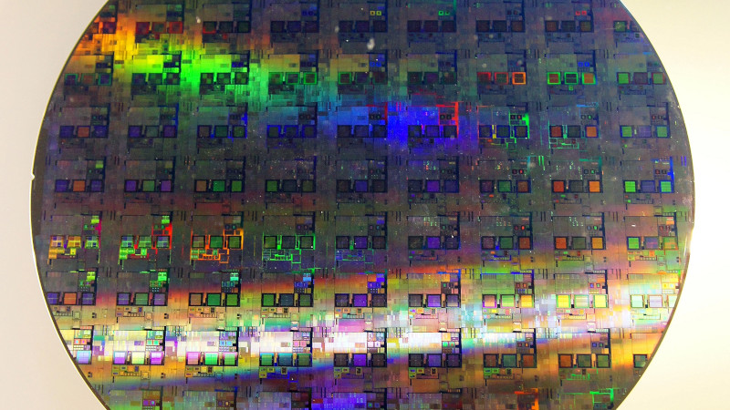
Notable about this process is that the 130 nm process being used isn’t cutting edge technology. The Skywater Technologies fab was built by Cypress Semiconductor in 1991 in Bloomington, Minnesota. Tim says professional designers have moved so far from these large geometries that our designers may have to rediscover some lost knowledge along the way to get the most from an IC made on the larger processes now. But the existing infrastructure is a big part of what makes this project more affordable.
So How Do You Get Them?
Tim had a lot to say about cell libraries that are eminent and how each one was tuned for a different purpose (e.g., high density or low power or high speed). However, we wanted to know how we’d get actual parts. Apparently, some of the details or still being worked out.
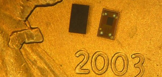
In November, they plan to order a multiproject wafer with 40 slots. They don’t know yet if they will have to beg and plead to get 40 designs or if they will have to winnow the select down from all possible candidates. If you are one of the 40, you’ll get about 10mm square to play with and wind up with somewhere around 100 to 300 chips in chip-scale packaging (CSP). You can see a typical CSP sitting on a US penny in the accompanying photo.
There are a few stipulations. You’ll submit your design on GitHub (or some similar public repository), so your design is going to be open source. That means even if you aren’t one of the 40, you’ve just put your chip out for the world to see. The foundry will automatically check your design to meet certain technical criteria. At this early point there doesn’t seem to be a firm plan on how they will select designs for inclusion in the first run. Presumably, if there are a lot of entrants and things work well, there will be more wafers in 2021.
There are still a lot of unanswered questions. Can you pay to get your own tape out? If so, do you still have to be open source? What if you have some made and then want more? How much does that cost? This is very early and we do we not yet know the answers to these questions, but details will come together over time.
The Key
Like I said earlier, ASICs aren’t for everyone and they certainly aren’t for people who test and debug as they go. Verification is essential for a successful ASIC project. That means a lot of this will hinge on the simulation tools available and the quality of the models available. Spending a lot of time and money getting ICs that won’t work at the speeds you need, consume more power than you expected, or simply don’t work is heartbreaking.
Many times an FPGA can be used to validate some or all of your design before trying to go to an ASIC. When that works, it works well. However, because of the differences between the two technologies, it isn’t as simple as thinking of an ASIC as a fixed FPGA. You have the same problems you might have going from a hand-wired circuit to a PCB. Logically they are the same. But we all know you can have problems with that transition because of the different characteristics. It is the same problem here. How do you test your analog cells? Will the clock distribute the same? And ASICs have speed or power requirements which are difficult to mimic in a validation stage.
Tim Ansel gave an online talk today officially announcing the project. Take a look for more details on the process node itself and the tools used to design for it:
So will you try to design your own IC? I’ve been involved in ASIC development before, but I still might be interested in doing my own personal project just to be able to do all the steps. Let us know what IC you want to design — or see someone else design — in the comments.
Header image: Peellden/ CC BY-SA 3.0


custom chips, it’s coming for sure, pretty, pretty good :) as i imagine we will have some open source (or free) fpga development environment with a cool dev board with a beefy fpga then after we are done with the verilog, we can send out the binary to make the asic, then we can select soic-28 for example and 15pcs and after a week or two we will receive our chips :)
https://www.skywatertechnology.com/
Wow! Right here in Minnesota!
So, how many transistors (BJT, FET, etc.) or gates, can be comfortably put on one of these 130 nm Chip Scale Packages?
(Rule of thumb)
I’m guessing some HaD readers have had (no pun intended, really!) some experience with raw silicon design.
To the best of my memory—and I’m trying to remember college classes from quite a while ago—an individual nMOSFET takes somewhere around 15ish square (process size). So if the individual dice are genuinely (10mm)², you have room for millions of transistors.
Mixing pMOS and nMOS does impose some extra overhead.
The AMD Barton (Athlon XP) has 100,99 mm² and 54,3 million transistors.
https://de.wikipedia.org/wiki/AMD_Athlon_XP#Barton
But a Pentium 4 Northwood as 55 million transistors at 145mm²
https://en.wikipedia.org/wiki/Transistor_count
Quite a lot, 5-10 million (minimal size) cmos gates or so. You can make a very non trivial digital ASIC on 10x10mm of 130nm wafer. Comparable to a Pentium 3 CPU…
Limitation will likely be metal layers, and IP for things like RAM. Of course you can make your own SRAM IP by copy pasting flip-flop circuits, but it will be less dense than one made by the foundry as they usually exceed drc, but get away with it due to the specific pattern.
I need to check this out. Very cool project.
SRAM is one of the easiest thing to make and most useful, so chances are that they are part of the standard library. Chip fabs uses it as benchmarks for their density. A decent grad course in VLSI would teach you how to build one.
As for making SRAM with F/F, your average F/F isn’t stripped down to 6T. :P You’ll have problem dealing with the fan in/out problems. The old MUX would add an insane amount of gates levels with lots of delays for any non-trivial SRAM array.
Modern day SRAM is connected up together with bit lines much like DRAM cells as that’s the only gate efficient way to deal with having a large amount of individual cells connected to a data bus.
I don’t think this is 10×10, this is more like 4×4 with 6 of those used up by the standardised harness (RISCV+RAM+Power+IOMux).
But using the P4 130nm example above of 55 in 145, you may still get 3.8 million transistors in the allowable area. But that’s if this 130nm process is even comparable to Intel’s 130nm in the past.
It’s likely enough to stick one of the Amiga FPGA designs inside.
Thanks for the replies, I’m impressed, but the Chip Scale Packages, are those tiny dots on the penny, not 100mm^2.
Leaving pads around the periphery for ohmic connections will cut into that real estate.
Build your own pun,
FOSSi chips v. Chip Foose.
I envision a dual processor chip: A linux capable core for ease of communicating with the outside world (tried and tested IP stack, support for basically all protocols, readily available and familiar tooling and such) that talks to the second core on the chip. That second core would do typical µC stuff like hard realtime und provide plenty of the usual interfaces (UARTs, I2Cs, SPIs, …) to talk to hardware.
If the interface between the two cores is well defined and strictly controlled, it should be possible to have a chip that is connected to the net while still having the important hardware control neatly separated. Which would be nice from a logical perspective and also for security.
So, a chip to build comparably safe IoT applications.
Most of the needed parts (eg. processing cores, slower hardware interfaces, all the software needed) should be freely available. A DDR interface of some kind might be hard to find, but would be needed for full Linux – I don’t see Linux on on-chip RAM in 130nm tech.
Also, would be nice to compare the available open source tooling and libs to what is commercially used.
There are some chips that fit that description – check out the Beaglebone Black’s Sitara processor, or the STM32MP1 line.
Thanks for the tips! I was aware chips like that existed (the Xilinx Ultrascale also come close, but substitue a µC core for an FPGA). But I wasn’t aware they were available in such ‘low power’ and ‘low price’ (relatively speaking) versions like the smaller STM32MP1 ones.
Realistically, for a lot of IoT or remote monitoring/managing applications, even the STM ones are already overpowered. Doing a similar concept on something like the google/skywater shuttle would ‘only’ have the benefits of proving it is possible on open tools / data and maybe add that single odd interface you need but noone bothered to put on a cheap off-the-shelf chip.
A true random number generator would be a chip for which open source down to the GDS might make quite some people happy, though.
And Freescale Vybrid. Also some of the i.MX families have a Cortex M4/7 for mopping up hard realtime tasks. Near full physical address range is available to both halves through a crossbar and Vybrid includes hardware semaphores in lieu of proper cache snooping.
An open source GPU would be cool.
Or something like a complete analog frontend for one oscilloscope channel on a chip?
Well, that’s beyond me skill level, but i would like to see it.
Well, here you go ;)
https://www.youtube.com/watch?v=l7rce6IQDWs
Okay, not quite a GPU but a first step
A single front end channel? Like a cut down version of the ADS54J66 , or the AD6649? I like the sound of that.
Keep the ADC sample rate below 150Msps to ease design constraints, more DSP power after the ADC, would create an impressive tool for students wanting to play with DSP in a real world setup.
I see 100 to 300 new 6581/8580 SID chips hitting the market in the near future. ;)
It would also be nice to recreate Amiga AGA custom ICs for the new PCBs.
Wouldn’t mind a quad POKEY DIP40 for my Major Havok boardset.
ZX Speccy ULA chips :D
My dream is to develop a wavelength-sensitive photodiode, an “one pixel spectrometer”. Silicon has an absorption spectrum such that multiple diodes stacked on top of each other see different wavelengths, as the short wavelengths are absorbed more strongly than long wavelengths.
There is an image sensor with three channels: https://en.wikipedia.org/wiki/Foveon_X3_sensor
But I am rather dreaming of a few more wavelength channels. Reading Wikipedia, the Foveon X3 sensor element has 5 um thickness, and in an 130 nm process, roughly 32 channels might be possible.
130nm is the minimal gate length of a MOS, not the substrate thickness. Which is around 500µm
I am into laser spectroscopy, but I have no clue on chip design. Thank you for the comment ! Do you think its feasible to put multiple photo diodes upon each other, reaching several micrometers structure thickness on the substrate as necessary for wavelength sensitivity from UV-A to near infrared ?
You don’t really “put the diode on” you build it up by masked layers of deposited semiconductors and insulators on the substrate, so each diode is a minimum couple of layers. So while it’s feasible to stack layers of diodes, it will also consume a lot of layers and layers = $$$$ so I’m not sure how many you’ll have to play with in a project like this.
I suspect there is a fixed layer count requirement. AFAIK it would not really be possible to build some chips on the wafer to say 10 layers, and others up to 30 layers, because the processing needed for the 20 layers after the first chips are “Complete” would affect the top layers of these chips. There’s some things like capping layers that can be done to mitigate some of these effects, but that would be quite hard to do on “one-off” wafers.
I don’t think open source silicon is really going to take off until someone comes up with a reliable maskless litho process (DLP based optical litho or e-beam seems most likely for the node scale offered here) with sufficient throughput. But it’s encouraging to see the first projects starting to get a footing and lay the basis. There are so many cool things that could be achieved with low part count custom silicon.
Betting poll on bran new C64 PLA, SID, VIC-II replacement chip dates?
Heck, let’s do the entire set.
Motherboards are already available.
Just stick it all on the same die so we can have C64
smartidiot savant watches.A bog standard nRF52 which can be found in quite a lot of bluetooth devices is already a lot faster than a C64.
Yeah it’s probably doable pretty much plug and play by blamming an emulator into one of those bluepill chips or something
its simple enough you can put it on small FPGA like Xilinx Spartan XC6SLX9 in ZX UNO that can do Speccy, Apple2, C64, MSX, CPC, NES and many more 8bits. Probably smaller FPGA is doable too. What we lack is new keycaps – a lot can be reused but few keys are unique enough, and we lack proprietary chips like C64 PLA, SID and VIC-II chips or ZX Speccy ULA (there are replacements on FPGA, and boards that don’t use ula at all), Amiga AGA and so on so the old systems with time die out for now theres enough of C64s and Speccys on market to salvage chips and repair boards in better condition but this source is limited and will dry out.
I’ve been dreaming about this for years, I’ve even done some layout and simulation with Electric VLSI and SPICE. I really hope this takes off!
https://chips4makers.io/ has similar plans, maybe with libre-soc https://libre-soc.org/
I hope to see a RISCV chip running Linux as soon as possible!
Difficult to beat a recent FPGA (typically <28nm) with a digital ASIC in (ancient) 130nm, at least for many things (especially complex things). For analog stuff (opamps, sensor interfaces, etc) – all is possible! Need proper models and design tools – as soon as that exists I strongly believe open source analog design could achieve a lot!
“Difficult to beat a recent FPGA (typically <28nm) with a digital ASIC"
Power.
Well, also depends on exactly what you're doing. 130 nm can push upwards of 1 GHz depending on what you're doing, and you can't run the general logic of an FPGA that fast.
But in general, I agree. 130 nm is a very solid process for analog designs.
Maybe we get a low power, trained, analog-based neural network object detector!
The 40 I/O restriction is a bit sucky. It makes it hard to come up with an idea that’s worth taping out especially when there is so much space available. There’s easily enough room for a Propeller clone + some exotic peripherals for example, but barely enough I/O to do a network interface while having enough left over for anything else. Might as well forget about having any sort of useful external RAM bandwidth.
The free RISC V thrown in for BIST is a nice touch though.
Transputer or XMOS network doesn’t take a lot of pins and can switch through a large number of processors if they have multiple ports. HyperTransport can scale down to 2-bits and as slow as 200 MHz per link. A 40-pin microcontroller that can talk PCI/PCIe through HT might be useful to someone. Might be more useful for sniffing a bus in order to perform tuning or diagnostics rather than being the bus master.
I’d hazard a guess at that process node, I/O speeds are going to top out at what, 100MHz maybe? :-/ Do they have LVDS even?
Pentium 4 (Northwood) was 130 nm and shipped at speeds of up to 2.2 GHz. Something much older like a Pentium MMX (P55C) was done in 0.35 μm and clocked at 120 MHz to 150 MHz.
Ultimately it will be design constraints that will limit you on speed over 100 MHz and not this process node.
You would need to have SERDES IP to implement something like PCIe. If their “free” library doesn’t come with that, you’ll need to license it.
The 40 I/O pretty much means GPUs, drop-in Amiga chipset are off the table. (OCS are on 48 pins)
JESD204B can pump a large amount of data over very few pins. Then there’s USB-C, USB 3.0, and… heck, even USB 2.0 has a (theoretical) 480 Mbps.
The problem becomes that of needing a 2nd chip, to decode and distribute the high speed data the 1st chip produces.
You’ll still need a SERDES to transmit or receive serial data no matter what fancy interface you are talking about. If you are using an external SERDES, then you’ll still run into the issue of burning up parallel I/O pins.
Something that have a fast enough PLL, control circuit to serialize parallel data and something with a fast enough receiver, clock recovery circuit to convert the serial data back to parallel. The serial data rate is such that it’ll be a lot of analog black magic, might include equilization, PLL and other things running at specified speed with little jitter.
Best project will be an Open Source FPGA, so no more reverse engineering of comercial designs. And use the existing open source synthesis tools.
You would very quickly run into patents owned by the big guys already in the FPGA industry. You think it is that easy to break into one?
There will be plenty of expired ones. A FPGA like 20 years before will be useful and the first fully documented one.
This reminds me of when BatchPCB first started. Real, professional PCBs! Hobbyists couldn’t dream to access those before without paying $$$$ and dealing with all sorts of logistical issues. And now it’s so simple and so unremarkable that you can get ten pcbs of ridiculously high quality in three days for less than the price of a meal at McDonalds.
This probably won’t go quite that far, but even if it gets partway it’s going to be amazing.
Tapeout in november?
I guess you better start working three month ago…
Actually you would need to have design working in RTL. 3 months is barely enough time to do the layout and any final tweaks before committing.
I wonder if chips on demand like we have PCBs now is feasable way to keep older FABs with old nm processes still up and running, i wish it would we could get replacement for retro stuff, and new interesting designs.
I request the Amiga chipset! Lol
The free RISC V in the library should be nice. Even the simplest version of it would be nice.