
If you were to travel back in time to the turn of the previous century and try to convince the average person that the grains of sand on just about any beach would be the basis of an industry worth hundreds of billions of dollars within 100 years, they’d probably have thought you were crazy. Aside from being coarse, rough, and irritating, sand is everywhere, and convincing anyone of its value would be a hard sell, unless your interlocutor was a real estate visionary with an appreciation of the future value of seaside property and a lot of patience.
Fast forward to our time, and we all know the value of the material that comes from common quartz sand: silicon, specifically the ultra-purified crystals of silicon that end up as the wafers we depend on to build the circuitry of life. The trip from beach to chip foundry is a long and non-obvious one which would not have been possible without the insights of an undistinguished Polish student and one-time druggist who discovered the process that made the Information Age possible: Jan Czochralski.
Those Who Can’t Teach
Born in 1885 in what is now Kcynia, Poland but was then part of the Prussian Empire, Jan Czochralski showed an early aptitude for chemistry. As always seems the case with chemistry prodigies, an early experiment in his home laboratory resulted in an explosion. His father, a carpenter, had aspirations that Jan would one day become a teacher, but despite his love of chemistry, or perhaps because of it, Jan’s grades were poor enough to preclude him from that career path. As an alternative, he left home and took a job in a drug shop, vowing only to return to his hometown once he had become rich and famous.
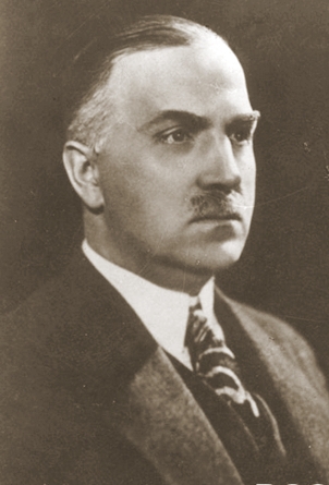
Jan continued his studies on his own and progressed through a series of jobs in Germany’s burgeoning chemistry industry. He was largely self-trained when he applied to and was accepted by the Technische Hochschule in Berlin Charlottenburg, where he would specialize in metallurgy. Soon thereafter, as a newly minted chemical engineer at the Germany electrical giant AEG, he began studies into the applications in electronics of what was then an exotic and expensive material: aluminum.
Czochralski’s career was advancing rapidly on the value of his metallurgical research and the degree to which he published his findings. His work was cited frequently, so much so that he would one day become one of the most referenced Polish scientists, no mean feat when the list includes names like Marie Skłodowska Curie and Stanisław Ulam. His fame was eventually such that Henry Ford would court him aggressively and offer to put him in charge of his entire factory in 1923. Czochralski politely declined.
Absent-Minded Professor?
For someone who was so driven and devoted to the field of chemical metallurgy, and for as methodical as Czochralski reportedly was, it’s ironic that what he is perhaps best known for, and the discovery that would certainly become his most important legacy, was the result of an accident. In 1916, as the story goes, Czochralski was making some notes on a metallurgical experiment at his bench. Intent on his notebook pages, he didn’t notice that instead of dipping his pen into the inkwell, he had dipped it into a crucible of molten tin. The story may be apocryphal, given that the melting point of tin is 232 °C and it would be unlikely that a careful experimenter like Czochralski would be so cavalier with a pot of molten metal, but however the pen got into the tin, the result was interesting.
When he withdrew the pen, a fine whisker of tin was drawn up with it from the pool of molten metal. Curious as to the nature of the thread, Czochralski analyzed it and was surprised to find that it was a single crystal. He continued to experiment with the technique, replacing the pen nib with various capillary tubes, and adding seed crystals to provide nucleation sites for crystal formation. He was soon able to produce single crystals of various metals up to 1 mm in diameter and as long as a meter and a half. In addition to tin, he used his method to produce crystal filaments of lead and zinc.
Czochralski duly reported his findings in 1917, and though there was an initial burst of experimentation by others into the “Czochralski method”, the distractions of back-to-back world wars left the work largely in obscurity. He continued working in the chemical industry for the rest of his life, and would live long enough to see researchers at Bell Labs — it’s always Bell Labs — rediscover his process in the late 1940s and apply it to materials he never imagined working with, like silicon and germanium, as they began to invent the semiconductor industry.
Planting the Seed
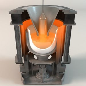
The details of the Czochralski process for producing the single enormous silicon crystals, or boules, that are the raw material of almost every semiconductor product made today varies from the original method only in minor details, and of course in the scale of production. Silicon boule production is carried out in an induction furnace that has precise temperature control and can be provided with an inert atmosphere such as argon. The process starts when a quartz crucible is charged with ultrapure (99.9999%, or one non-silicon molecule in a million) polycrystalline silicon. The furnace is heated to about 1,500 °C while the crucible slowly rotates.
When the polysilicon has melted, a puller rod is lowered into the molten silicon pool. The end of the puller rod carries a seed crystal of silicon in a precise orientation, to serve as a nucleation site for crystallization. The puller rod, which is rotating in the opposite direction from the crucible, remains in the molten silicon for a short time before slowly being withdrawn. The molten silicon has by this point started to crystallize, and the puller rod begins accumulating a cone of crystalline silicon in the same orientation as the seed crystal.
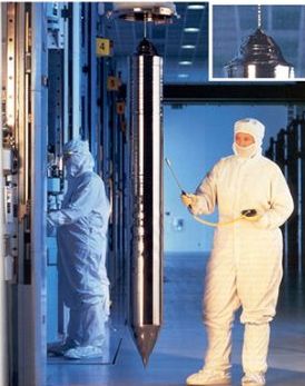
Eventually the growing crystal reaches its maximum diameter, and the boule becomes more cylindrical. The diameter of the boule can reach up to 300 mm routinely, although 450 mm diameter processes are currently being prototyped; a theoretical maximum of 675 mm is possible but has not been attained. The boule continues to grow as it is withdrawn, a single crystal of silicon dangling from the puller rod and eventually weighing several hundred kilograms. The video above gives a good overview of the entire process, from production of polycrystalline silicon from quartzite sand through boule formation, and on to the fascinating details of processing the boule into wafers.
Not Just for Silicon Anymore
The Czochralski process is not only used for silicon crystals. Synthetic gemstones, including ruby, sapphire, garnet, and spinel can be grown using the method. On the other hand, the method is far from the only way of making ingots of monocrystalline silicon.
The float-zone process, also developed at Bell Labs, uses RF energy to heat a zone within a rod of polycrystalline silicon. It can produce silicon of much higher purity since the melt isn’t exposed to oxygen by the quartz crucible of the Czochralski method. There’s also the Bridgman–Stockbarger method, which is basically an upside-down version of the Czochralski method.
At the end of the day, though, Jan Czochralski’s accidental discovery of a crystal-growing technique has stood the test of time, as something like 90% of silicon wafers are cut from boules grown using his method.


“coarse, rough, and irritating”
As a youngling I disapprove of this comment…
Duly noted.
Still waiting for hackaday to feature an article on a homebuilt Czochralski furnace for growing ruby boules.
I could use one for making large batches of watch jewels, Though I doubt any normal person has a need for one.
Yeah, I know there was the one article on making a ruby, but it really didn’t make one properly like this method can.
I thought maybe the homebrew laser people would have had a crack at it, but I couldn’t be arsed fighting google for more than a couple of tries. I did have a googlefu blackbelt but it’s artificial stupidity is 3rd dan now, so gotta put in some training.
Hear, hear about Google. Even “search strings” in quotes have long since stopped working properly.
Right, just give me stuff with the actual keywords in and stop trying to guess what I mean FFS.
Always a mark of immense species-wide shame when I discover I can coax Bing into delivering more relevant search results than big G
“As always seems the case with chemistry prodigies, an early experiment in his home laboratory resulted in an explosion.”
Isn’t that usually the goal?
New YouTube channel needed: ChemicalBOOM, to go along with ElectroBOOM. Ponderous eyebrows optional, as they’d probably get burned off anyway.
That’s what Beaker™ was for.
Meep meep mep meeeeep?
I’d be pissed if I pursued Chemistry and just got plain ol’ cancer instead of annihilated in a rocket fuel lab explosion. Or meth lab. I’m not that picky.
Depending on the chemicals you play with, you could end up with one of the more exotic cancers…
If you’re real careless like that, you either end up hailed as the inventor of saccharine or a disturbing number of artificial sweeteners and flavors… (Hmmm this tastes like bananas, etc) .. or dead from stuff the coroner can’t identify.
Either way, they get something named after them.
“Still waiting for hackaday to feature an article on a homebuilt Czochralski furnace for growing ruby boules.”
I second that.
Similarly, I’m motioning for an article on growing crystals for optical an other electromagnetic applications. Maybe even a DIY Disco slicer thing-a-majigy.
Processing the materials is even worth an article.
Ah, man, like I don’t have enough on my plate already.
Sighs, adds yet another project to list…
You have have it sport! That’s the spirit! :-|)
Agreed, Have been wanting to build one since I was 10 (that was a very, very long time ago). Have collected a few parts along the way but with higher power devices becoming more easily available (or scroungable?) maybe the furnace power supply might not be too tough to get started? I mean who doesn’t want to melt stone in such a cool way?
Seed crystal surface orientations are what the real issue for me,I just don’t get it from what I have found to read on it, so maybe an article on that (or a link).
Part of a series of articles on the project…… just a thought, might only a few of us…
but then after that who wouldn’t want to try to build a small shop size controlled atmosphere induction metal melting furnace / pouring station for inert atmosphere for melting and casting magnesium, bronze, ss alloys (maybe the first one should be outside the shop)……
Surely there are folks here who work on or for some company 5hat has made induction heaters before, or someone has made one before.
I would think making ruby is something someone would jump at, just for cool factor and technical challenge
God I wish this site had an edit function already.
Don’t remember finding one here, only project one I remember finding would heat a large bolt red hot, wrong frequency, and not enough power. And of course ruby was the goal (it was a few years after the ruby laser was invented).
I thought you had found a new spelling for “phat”, but then realized that it didn’t fit in the sentence.
I used to do this for a living. It was a very nice article to read it was like a real flashback to the 80s. Are used to work for a branch of Rockwell international and believe it or not Pottstown Pennsylvania, and we made silicon wafers out of raw wacher or dynamit Nobel silicon. Before I worked there, they actually made wafers to supply to Commodore computers, which was down the road in Norristown right next to Valley Forge, and also in West Chester Pennsylvania.
As far as finding the proper seed orientation etc., I am very sure you can shop around and look for them sold in the industry, since you’re using relatively pure silicon with a few additives of different types of metals or materials to the melt, I’m pretty sure these companies at startup Use a pure supplied piece of silicon of a certain orientation. But the way we made them was we would actually grow a seed crystal which might be a few inches wide and 30 inches long, and it would be grown from an already existing seed crystal. When this was processed, it will be taken to a grinding department, where the outside will be ground off and one of the required steps in the grinding process would be the application of x-rays to the Crystal at different points to make sure that it was in line within whatever parameters of degrees to the orientation that was being sought.
So during the grinding process, the grinder would grind and cut the seed to a certain specified width and shape sometimes round sometimes square to fit the truck that was in the upper chamber of the furnaces that we grew the silicon crystals with. So say that you had a 111 or 100 Crystal, there were many different orientations sometimes experiment with some very weird orientations 110 etc., But the grinder with x-ray to see the different points making sure that the seed when I came out of the bottom of the check was gonna be 100% on to pull out a crystal of the orientation that was needed.
What I’m basically getting too, is that all you would need to find is a relatively pure and high-quality seed stock or Crystal stock, which I’m sure there are many of them existing in the world, But the grinder with x-ray to see the different points making sure that the seed when I came out of the bottom of the check was gonna be 100% on to pull out a crystal of the orientation that was needed.
What I’m basically getting too, is that all you would need to find is a relatively pure and high-quality seed stock or Crystal stock, which I’m sure there are many of them existing in the world, and get an x-ray machine to measure off of the plane of the particular orientation you’re looking for and then cut according to that.
Or just order a seed stock from a silicon crystal house somewhere which I’m sure they still exist. I didn’t bother yet to look up on eBay. Also I should mention the types of furnaces we use for the most part back in those days, were Siltec and Hamco, and I’m pretty sure those still exist in place is industrial sales yards etc., but be aware those old tanks and those old jackets of the cooling tanks that we used used to some of them went through a lot of traumatic experiences water shut off‘s etc.
One funny thing I thought that wasn’t mentioned in this process was that when some of the engineers for some of the new furnaces that we bought at one point came to set up the furnace is in our Department, we were talking to them about how small time our operation was, And they made reference to places they had gone to install them around the world, where they said that actually someplace is the shipping crate that the furnace came in or was shipped in was the majority of the “building” which the furnace would reside in. That was hard to imagine, seeing how these machines required so much electricity to attain the levels of heat that they did, and the conversant level of cooling water etc. to maintain operation. I should say to that a lot of these furnaces had two parts the main tank part that the silicone was melted in side of etc. and the gas is in the flow within that and then a completely separate control panel that Adjusted the orientations the speed of the ball running inside of it the speed of the app seed rotation and speed of draw out of the crystal etc. to be honest with you it’s one of the most fascinating processes I’ve ever had the chance to witness. It’s too bad the companies back then didn’t pay more money and respect their workers more it was a very low in type of operation.
I should’ve mentioned, that one of the critical factors about the seed you would use is the type of material that you’re creating in the crystal your growing relative to the type of seizure using like as it says I’m sure in this article it in these videos they were acceptor and donor type materials used in the dopants meaning you have a P tape or an M type basically of silicone that’s produced. So the last thing you want to do is use the opposite type of seed in a melt or growth. It probably wouldn’t matter if it was a virgin type of seed grown out of a another Crystal because most people wouldn’t you seeds that were had a very high amount of dope and in them because that would in itself give a certain resistivity or a treat to the resulting Crystal you don’t want that you wanted the Crystal to be created out of the dope is that you add to the pier silicon himself just the two of them. But a lot of the seeds and a lot of the crystals that or see you might use from a certain already pre-ground Crystal would have so little dope and in it to begin with if it was say a very high resistivity Crystal if it never had very much dope and it probably wouldn’t matter too much but you want to make sure that you use the right Type of seed with the right type of doping you’re going to add any type of P tape and within a certain resistivity range things like that
How does crystal orientation affect the wafer and the circuits built on it?
I had a former cow-orker that previously worked in X-ray crystalography in the Research Triangle of North Carolina.
It’s like the first layer of bricks, if you start with herringbone, it continues with herringbone, if you start with a stretcher bond it carries on with a stretcher bond.
My admittedly poor understanding of crystal faces is that for electronics, each different face may have its own set of atomic and electronic properties, as in certain faces may exhibit better atomic alignment/matching for the next layer to be added/deposited in the “wafer” stage by epitaxy or CVD, and possibly for etching, and for electronic properties as conductivity etc. As this is truly far more complicated than making “optical” crystals such as ruby (chromium doped alumina) or YAG for lasers it was never in my sights… I think the purpose for laser crystals is to obtain the correct orientation required for the crystal (in the case of ruby at least IIRC) is to accept the pumping light from XENON lamps along the long axis and bounce back and forth between partially mirrored ends to produce “gain” before leaving the “front” of the crystal at the characteristic coherent frequency. I believe there are “optical” methods for this that do not require X-ray machines as for the much more complicated electronic components, though the furnaces operate in the same way, higher frequency generally for melting oxides like alumina, lower frequencies for “metals”. I believe 60 Hz can heat iron but ~900 Hz or higher for alumina. For conductive / magnetic materials I believe eddy currents heat and stir the melt. Not clear to me whether the melt material or the crucible transfers heat to non conductive / magnetic materials at the higher Hz.
Are we posting AI-generated nonsense now? Guess it was only a matter of time …
They aren’t posting nonsense- I know and follow what is being discussed.
Nice to see such details from someone who did it for a living- some might see this as a rant, I don’t. Though this doesn’t help much with my type of basic ruby- because there is no doping needed for that nor any p or n type to the melt.
Basically, the reason this specific method interests me is because the melt crystal has no internal stresses compared to flame fusion (which can be done at home), and I need a very specific hue of red, and other colors, to do what I want with my jewel bearings, that is easiest measured and repeated with this method of melt, as well as most optically pure compared to flame fusion.
Nobody would have guessed that Mr. Czochralski’s process would have started an industry worth a trillion dollars.
But Mr. Czochralski died before that happened. The world didn’t see silicon turn into microchips until he was in the ground for a decade.
In the ground? really? I would have expect him to be cremated
Back when I was at the university we used to grow scintillating calcium tungstate (CaWO4) crystals via the Czochralski method. The crystals were used to build dark matter detectors.
https://www.cresst.de/crystalgrowth.php
The Czochralski technique is one of the most common production method for inorganic scintillators which are widely used in particle and nuclear physics experiments but also e.g. in PET scanners. A prominent example is the CMS calorimeter which consists of nearly 80,000 lead tungstate (PbWO4) crystals which were grown by the Bogoroditsk
Techno-Chemical Plant in Russia using 150 Czochralski ovens. A lot of the expertise for crystal growth still lies in former Soviet Union states.
I also once visited the silicon fabrication at Wacker Chemie in Germany. What totally amazes me is how they are able to dangle a several hundred kilogram heavy ingot from the thin seed crystal as shown in the picture above.
Hahaha, good one Ren. Don’t you know, all matter matters!
You know any noun can be replaced with a verb, because nothing exists as a thing in itself, but a happening.
Just close your hand and you are fisting!
I’ve long had a dream of making single-crystal rock candy. Too lazy to try, but at least now I know the name of the method.
That’s easier, you can do it from a solution, you don’t need to have it at melting point. Melting and catching fire are kinda close together where sugar is concerned though, so a decent candy thermometer and a very controllable heat source would be recommended if you want to try it the melty way (Which I’m not sure works anyway, molten sugar is more like a glass I think)
Interestingly, these crystal ingots were not usable for making transistors and ICs as grown. They had to be refined further, using a process called zone refining. Gordon Teal at Texas Instruments figured out how to do this in about 1954. Naturally, he got no initial funding and had his oven set up in a hallway, according to the lore. I have no idea how they do this nowadays though, because I don’t work in the industry.
“… using a process called zone refining”
Reminds me of this series that details the history of the electronics industry in Japan and their refining methods at this time (~ 19:15):
https://youtu.be/ihkRwArnc1k?t=1156