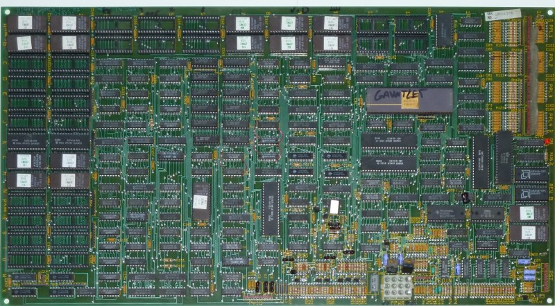
Gauntlet is a well-known arcade game from 1985 with many sequels and ports to more modern architectures such as Xbox and GameCube. Thanks to its popularity and relative age, the original arcade cabinet is well documented with the schematics available online. It was regarded as the most complex and ambitious hardware Atari had ever developed at the time it was released. In what can only be described as an absolute labor of love, [Alex] has recreated the arcade hardware on the Pipistrello FPGA board.
The project can actually play Gauntlet, Gauntlet II, and Vindicators II as they all ran on the same hardware. Four joysticks are supported so up to four players can play, though the EEPROM is emulated in RAM so high scores are reset when the device is powered down. The FPGA is almost out of space and can’t quite squeeze in the SRAM needed. So an SRAM expansion daughterboard is required; nothing a quick board run from our favorite purple PCB manufacturer can’t solve.
In the repo is an incredible write-up detailing the system, how it works, and the process of debugging it. This project also includes a complete simulation of the TMS5220 Voice Synthesis Processor, as Gauntlet was the first coin-operated arcade machine with a voice synthesizer. Getting the video correct was particularly tricky and it took several tries to get the color palette and motion looking right. Since [Alex] didn’t have access to an original Gauntlet arcade cabinet, they had to make do with MAME. After writing a test to make sure the FPGA was working correctly, there were differences between the MAME emulation and the FPGA output. To help out, [Colin Davies] came to the rescue. After [Colin] hooked up an original Gauntlet Arcade PCB with the motion test loaded up, the test showed that the FPGA had the correct behavior.
During development [Alex] actually simulated several frames of the game in ISIM (at a whopping 90 seconds per frame or 90 minutes per in-game second). Using ISIM allowed them to compare system state to MAME and validate the design much faster as they could better inspect the interworkings of the different modules. Using a clever trick of grabbing state from MAME after a few seconds, they primed the FPGA state and saved themselves a few hours of simulation.
If you’re looking to get into old hardware style arcade game development, give the browser-based 8bitworkshop IDE a spin. Or start with something a little smaller in scope and size with this adorable mini CRT arcade cabinet.
Thanks [Alex] for sending this one in!


Gauntlet wasn’t the first game to speak. Berzerk was speaking in November 1980. Stratovox is billed as the first video game with voice synthesis, released in May 1980. Wizard of Wor also spoke, coming out in December 1980.
indeed the first atari system I board also implemeted the same speech unit but on the A3 sized cartridges :)
the system I and later II were some of the earliest advanced coinop designs, used by military as well for simulation.. A behemoth of a motherboard dimensioning some 500X800 mm minimum.. ahh, the days
You beat me to it. From a Google search, it seems Gauntlet was the first Atari arcade game to have voice synthesis. For some reason, others have morphed that into the statement that it was the first game of any manufacturer with voice synthesis, which is wrong.
Came here to say this. I was also going to mention Gorf, but after checking its release, discovered it didn’t comeout until 1981.
As far as actual history goes regarding speech synthesis in Atari arcades, it is noteworthy to mention that Texas Instruments introduced the TMS5100 chip (known internal at TI as TMC0280) which was a LPC (linear predictive coding) speech synth which was used in the Speak and Spell game demoed at CES as early as 1978. Eventually the TMS5100 chip was further developed and released as version TMS5200 and then TMS5220 in 1980 then TMS5220C in 1983. So it is the TMS5220C that can be found used on Gauntlet arcade games PCB, see https://en.wikipedia.org/wiki/Texas_Instruments_LPC_Speech_Chips as reference.
“Don’t shoot the food”
“wizard,, is about to die” zz zz
funny memories
The video in the article is of an earlier development phase. The game is now fully functional and can also run on MiSTer.
Seems like the project could use some more documentation. What kind of input is used? Perhaps also provide a few pointers to someone would like to build this but doesn’t know what tools to use.
Hi, thanks for the feedback, I do mention Xilinx ISE 14.7 and Quartus 17 which are the “tools” you speak of. There is a certain amount of basic knowledge one must have if they choose to compile the source code themselves, such as install the tools, double click on the project file and click compile. Additionally the ROMs are Atari IP and are not provided in the source code so one must figure out a way to obtain them and convert the binary files to VHDL, I think anyone having trouble compiling this project needs to start with something simpler first.
For newbie users the MiSTer platform is recommended as the core is provided precompiled. Since the MiSTer platform is more widespread and has an active community, the inputs are “taken care of” through a standardized interface common to all arcade cores and also customizable by the user through an on screen menu. There’s not much to do once you’ve downloaded the core and the ROMs to the MiSTer SD card other than select it from a menu and start playing.
The Pipistrello, being more of a one off, experimental board, it is up to the user to figure out a way of connecting the inputs and compiling the source. In my particular case I only had one player control connected to one of the PMOD connectors which allowed me to hook up a gamecube controller and play single player during testing. I don’t see the now discontinued Pipistrello being the board of choice for the vast majority of arcade builders.
What is this MiSTer thing of which you speak? Looks like a bear to search. Link please?
https://github.com/MiSTer-devel/Main_MiSTer/wiki
Wish I had his perseverance! Love FPGAs for what they can do, hate using the snail paced tools to get there. Meanwhile, this dude doesn’t mind running 90 seconds / frame simulation to see where he is …
currently at work we’ve got a sim that takes 20hrs to simulate a 1sec rf transmit and receive cycle. It’s definitely an inhibitor to progress, and a pain in the ass to verify things.
Atari Star Wars had a speech synthesiser in 1983. Actually it was used to replay samples from the film.
It used the same chip. The TMS5220.
I don’t get where all the RAM requirement is coming from. I haven’t dug too hard through the design, but it has to be that the ROM is being loaded from flash into RAM, and then run that way? The RAM on the FPGA is huge (2 MB), there’s no *way* there’s that much RAM on an actual Gauntlet board.
m68k’s have a 4-clock bus sequence: address-to-data valid, at 7.16 MHz, is ~350 ns. In XIP mode in quad I/O, it takes 10+dummy cycle count for an arbitrary 16-bit read/write (6 address, 4 data). Considering the ROM only covers a 20-bit space, if you align it properly the first clock’s free, too. At, say, 12x system clock (85.92 MHz), you’ve got 30 clocks from address -> data, and you only need 18 to get it (8 dummy cycles at ~90 MHz). That’s a *lot* of margin to work with.
Hm. Might have to play with this.
I think you need to read the datasheet more closely. The SLX45 has 2M *bits* of BRAM, in 18 bit wide blocks. There is 64MB of SDRAM on board of the Pipistrello, but for some reason the FPGA retro computing community don’t seem to be in a hurry to use SDRAM.
Nah, I just need to be more careful typing: it should’ve said 2 Mb. Considering system RAM’s 64 kilobits and video ram’s something similar, that’s why I said no way it needs more than 2 Mb. 2 Mb is a huge amount of RAM for a vintage 80s console!
The reason DDR’s not used is because of the indeterminate latency due to refreshes/page accesses. If it’s fast enough, it seriously doesn’t matter, but this isn’t high end or anything.
But using the SPI flash in quad I/O XIP mode is an easy trick for sub-8 MHz processors that gets overlooked a bunch.
The FPGA community is a very broad statement so I guess you’re mostly right, the reason being is that interfacing to SDRAM is hard. Having said that, the MiSTer community is definitely using SDRAM in many arcade cores and I too am looking into ways of leveraging that for this game. One thing many don’t realize is that while modern DRAM including DDR is very fast at streaming sequential blocks at multi Gbps speeds, it is absolutely _crap_ when used to fetch non contiguous _words_ as is the case in an arcade.
For every word you need to get out of the DRAM you need to activate the row, wait some clock cycles, supply the bank and column adddress, wait some clock cycles, read the data, (auto)precharge to close the row, wait some clock cycles then repeat that entire process for a whole another non contiguous address. On top of that you have that pesky thing called refresh, so every so often, usually at the most inopportune time when you really really need to read some data, the refresh timer expires and you have to issue a refresh command then wait some cycles for it to complete.
Compare that with the 10ns access time of the SRAM used on the custom daughterboard with the Pipistrello. Place address on address bus, after >10ns read data from data bus. Done. Repeat for other addresses. You can read all the ROMs for video, audio and main cpu and have time to drive to the shop and buy some milk in that time before the next clock cycle arrives and you have to do it all again.
Many early arcades were designs with a multitude of ROMs connected to different parts of the circuit, in this game you have video ROMs, audio CPU ROMs, main CPU ROMs, character generator ROM, and they are all accessed simultaneously (with video ROM accessed double time so it fetches both sprite data and background tiles) so a fast SRAM is literally a godsent. Once the game is fully debugged one can start looking into the timing requirements, caches, etc, needed to move things into an external DRAM.
“On top of that you have that pesky thing called refresh, so every so often, usually at the most inopportune time when you really really need to read some data, the refresh timer expires and you have to issue a refresh command then wait some cycles for it to complete.”
For emulating older things, the easiest thing to do is just interleave a refresh cycle after the access. Old DRAMs (not SDRAM, the stuff on SIMMs back from the early 90s) are actually really handy for this if you can get the fast stuff (50 ns access time). Do a hidden refresh each cycle. You get data within 50 ns so long as you don’t need to access it again within another ~200 ns.
For ROMs, if you’re careful, you can get fast SPI (the 133 MHz guys with quad I/O support) to give you ~100 ns latencies or so for ROM size up to 1M (again with full cycle times of 200 ns). You preload the command and drop the 1st nybble, use as many of them as needed in parallel (4 bits each), and you’ll get the data *barely* around 100 ns.
And if you’re wondering why that ~100-ish ns value’s so important, check out the Nintendo Developer’s Manual on an SNES’s FastROM timing. :)
Famous last words “I haven’t dug too hard through the design, but… there’s no *way* there’s that much RAM on an actual Gauntlet board.” made me LOL
Gauntlet uses 256KB for video, 48KB for the 6502 audio processor and 160KB for the 68K.
Vindicators part II is even worse, 768KB for video, 48KB for the 6502 audio processor and 352KB for the 68K.
These are just the ROMs, not counting the RAMs needed or the Char Gen ROM too.
Yeah. By “dug too hard,” I just meant I read the Gauntlet documentation, dug through the HDL files but didn’t try to actually connect things because the repository’s not really organized well and the HDL’s written more in terms of the schematic. Which is neat in some sense, but freaking awkward to poke around if you’re not super-familiar with the schematic.
“but… there’s no *way* there’s that much RAM on an actual Gauntlet board.” made me LOL”
RAM. Not ROM. As in, random access memory. As in, the expensive stuff, things you can write, stuff that actually requires large amounts of transistors, as opposed to “burn a bunch of fuses with high voltage and sell them for pennies.”
ROM you can handle with the SPI Flash. RAM, obviously, your only other alternative is DDR, but for that you need to ensure you can offload refreshes deterministically. And that the DDR’s fast enough. Not impossible, but not easy (and the Pipistrello’s DDR is fairly skimpy).
From the documentation, you’ve got:
1) 8K off the 68010.
2) 4K off the video.
3) 4K color RAM.
4) 4K off the 6502.
That’s basically what I was able to track down in the HDL. Plus maybe one or two others, but nothing serious (which again, is what I’d expect – SRAM was crazy expensive in the 80s). The 6502’s program ROM would likely need to live somewhere else, but it’s *so* slow that the DDR4 might be best for that. Even still, 48 kB isn’t *that* bad to bury in the block RAM.
The answer to my original question, though, is that you *really* need that much RAM for the graphics ROMs, because they’re asynchronous and run at clock. There’s pretty much no way to avoid that, since at that point you’ve got ~100-ish ns to complete the transaction, and there’s no way you can mimic that with flash or DDR.
“the repository’s not really organized well”
I should clarify “not organized well” should really be “not organized the way I’m most familiar with.” Given the godawful way that most FPGA development tools interact with repositories there’s not really a “good” way to do it. Although I will say that with a design in VHDL, I *super* recommend using something like VHDocL or Doxygen.
Well the beauty of open source is that it allows you full access to experiment with the source code. If as you said you’re confident you can get away with running all the ROMs off the serial EEPROM then give it a shot.
I know the diff. between RAM and ROM, but in my world of arcade simulation and given the hardware available, all memory ROMs and RAMs eventually end up in a RAM, whether static or dynamic, inside or outside the FPGA, so I count all memory in terms of RAM memory cells.
The MiSTer platform which is based on a DE10 nano has a SDRAM which is shared with the HPS ARM cores in the FPGA and is generally accepted it has too high a latency to be useful for fast random access. Additionally there is a custom SDRAM board dedicated to the FPGA and it is this that I’m looking at utilizing in order to fit all the ROMs so that Gauntlet II and Vindicators part II can also run on MiSTer (all these games run already on the Pipistrello with the custom add on SRAM board so I never invested time to get the LPDDR going on that).
I love the Atari Gauntlet games and I’m happy I can play them on an accurate reproduction of the hardware rather than emulated in MAME, especially as custom LSI Atari chips become harder to find as they fail due to age. As described in my debugging section on github I already found discrepancies between MAME and running the games on the FPGA. These differences may not be significant but any purist who has played the original back in the day will recognize the differences, one such super obvious example, the sparkles during screen transitions caused by the hardware interactions, these are not visible on MAME.
“Well the beauty of open source is that it allows you full access to experiment with the source code.”
Yeah, although, again, the complete lack of standardization of any FPGA tools means it’s a massive pain. I need to port the design over to Vivado since I can’t spare cycles working with dead FPGA tools, which means shifting to a 7-series board (probably an Arty-A7 or a Zedboard, or one of those $20 AntMiner boards). Which sucks, since it means rebuilding the project and simulation set. Joy.
“If as you said you’re confident you can get away with running all the ROMs off the serial EEPROM then give it a shot.”
No, I can’t, not on that board. That’s what I said. The difficulty isn’t the *amount* of ROM needed, it’s the fact that you need multiple paths (so you can’t do it with 1), and one of them has aggressive timing anyway, so you’d need a faster SPI flash than what that board has, anyway.
I can *probably* sleaze it with an additional add-on board which uses multiple SPI flash chips instead, though. Or compress it, or super-sleaze it with DDR. I just need to stare at how the graphics stuff is handled – obviously since they’re piped through a shift register, you can likely do super-sleaze cheats (like precache just the first bits of everything and then catch up on the rest once it’s available).
Hm: that last part sounds more tractable: 256 kB sliced in 8 is tractable in the FPGA itself.
“but in my world of arcade simulation and given the hardware available, all memory ROMs and RAMs eventually end up in a RAM, whether static or dynamic, inside or outside the FPGA, so I count all memory in terms of RAM memory cells.”
Yeah, I’ve noticed this pattern among other people, too. *Really* don’t understand it. A ROM being read-only offers *so many* more tricks that you can pull. I mean, you want to hide refreshes? Use two memory devices and toggle between them. Poof! Refresh issues gone. To be honest it’s *incredibly* easy to just go and salvage off old 3.3V EDO DRAM chips, and pair them up. But that’s so easy it’s not worth the challenge.
There’s nothing you can do about *actual* RAM, so it’s super-important to distinguish the two. That’s what started me down the whole rabbit hole, anyway – I knew it couldn’t be *actual* RAM that’s the limitation, which meant it was just a question of the latency requirements and the datapaths. The program code for the processor is easy to handle, the difficult part’s the graphics ROM.
OK, the graphics ROM is going to be trivial to put in RAM. Even after the address is first made available, you’ve got ~535 *nanoseconds* before it’s used by anything, and then because the graphics update cycle is only 50%, it’s a *microsecond* between accesses. Again, not terribly surprising given the age: the address is out on clock 1, data loaded at clock 4.
That’s an *eternity*. DDR can handle that without any problem.
Also, as I thankfully hoped, Vivado is about 3-4 times faster than ISim, so “hour-long simulations” aren’t a problem.
COVID-19 idleness lays another egg?
When I started this project, COVID-19 wasn’t even so much as a glimmer in its daddy’s eye. Ahh the good old days…