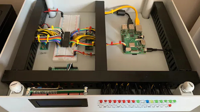
The Z80 was a big deal in the 1970s and 1980s, and while its no longer a dominant architecture today, its legacy lives on. [James Andrew Fitzjohn] is a fan of the Z, and decided to interface the real silicon with the Raspberry Pi, by and large for the fun of it!
The Z80’s address and data lines, as well as the clock, are hooked up to the Raspberry Pi through several MCP23017 GPIO expanders. The Pi’s GPIO lines aren’t known for their speed, of course, and using expanders through I2C isn’t exactly quick either. However, speed isn’t necessary, as the clock only goes as fast as the Raspberry Pi desires, since it’s controlling the clock along with everything else. There’s also an LCD for viewing the Z80s status, along with some era-appropriate blinkenlights.
This setup allows the Pi to run code directly on the Z80 itself, while managing the CPU’s RAM in its own memory, all through a Python script. It’s a fun hack that lets you run retro code on retro silicon without using an emulator. Techniques like these are useful for finding undocumented or edge case performance of a processor. If this hack isn’t enough Zilog for your liking, consider throwing one in your pocket as well!


Lovely hack. Absolutely useless, in the practical sense, but has amazing teaching potential.
The Z80 was a great processor, in the day. I still have a few SBC’s around that run Z80’s (original Z80A and NSC-800) from back when I was just out of UNI and doing custom hardware (career number two of five(?) so far).
Love to see Z80 projects! It’s way before my time, but got a batch recently and enjoy tinkering with them.
The case is lovely. The wiring is tidy. Clearly much effort was put into this. But the construction is solderless breadboard? Is that really meant to be permanent? I’ve never used a solderless breadboard long term. If you come back years later does it still work? Or does everything need pulled out and re-inserted to clean the contacts? If you store it away and it gets knocked around a bit or if it gets stored upside down then you come back and try to use it is it still good? Or do connections come lose?
I’m not trying to be mean. I’m just curious. I’ve seen it here before but I just can’t wrap my head around the idea. Maybe it’s generational. When I started a breadboard like that when adjusted for inflation would have probably been $60 or more in today’s money. Once working, moving to PCB was a necessity because you needed your breadboard back for the next project!
Thanks! Glad you like the case, it took a lot of swearing and time to get the LEDs lined up. I will be creating a custom circuit board to make it all easier but i’m still trying to teach myself CircuitMaker
Very neatly executed project.
I’d like to see it go a step further and to be used to test clock speeds (perhaps programmable clock) that the chip fails at for various (undocumented) instructions.
Back in the day I used to program in machine code as I didn’t have an assembler.
To do this I printed out 4 sheets of instructions and their op codes formatted on a 16 by 16 table. The x number of the table element was the second hex value of the instruction and the -y value was the first hex digit. I did this for convenience to fit to a page. Some instructions were in groups of 16 but most were in groups of 8.
The first table was the base set of instructions and the other three tables were the extended sets.
The instruction mnemonics weren’t hard preprogrammed strings but rather decoded from the hex value.
This was the understanding I needed to write a disassembler.
The instruction decode logic was immediately obvious in the tables. And so it immediately became obvious what the undocumented instructions where.
The one thing I have never realized is why the undocumented instructions were never documented. I never had any problem using them.
The story was that the instructions where toward the edges of the die and therefore had greater propagation delays and that would cause problems at higher clock speeds.
It would be interesting to put a programmable clock and small CPLD/FPGA between the Pi and the Z80.
A small CPLD or FPGA would have enough RAM (as LEs) to run the small number of bytes to execute a specific instruction (at various speeds) and read back the CPU status (register and flags) to see what it’s failing point is.
I would expect that original Z80s date stamped from the 70’s / 80’s may fail with undocumented instructions at in spec speeds and more modern equivalents (Z84C020) would no problems at all or perhaps some problems with undocumented instructions when over clocked.
It would be very interesting to know the answer to this question.
If your interested, suitable CPLDs that are still available and 5 volt tolerant would be Altera EPM240/EPM570 (approx 240 and 570 equivalent LEs) or Xilinx XC9536XL / XC9572XL / XC95144XL (36 / 72 / 144 macros). A LE is about half a macro so the Altera would be better choice. The Altera datasheet says to use series resistors for 5 volt tolerance but I have never used these series resistor and have never had problems.
Thats interesting about the undocumented instructions, I had always assumed that under certain circumstances they could do unpredictable things… not that the actual silicon couldn’t work reliably at speed.
An external clock would be “interesting”… the GPIO extenders are really slow and they love holding the i2c clock low until they are good and ready, open to ideas on a faster bus/getting them synchronised though.
Well that’s the question that I haven’t answered.
You said “under certain circumstances they could do unpredictable things”
The “certain circumstances” implies that there is some predictability.
As for clock speed, things are different for different chips. For example the common ATmega328p will easily run with a clock above 30MHz at room temperature and 5v Vcc. But it will only do so with an external oscillator. The internal oscillator can’t run that fast but the rest of the chip is fine at higher speeds.
It would be a bit of a squeeze to do this with a 5v CPLD like the EMP570 and it wont be able to emulate much RAM. You don’t need a lot of RAM so it may be doable.
I’ll mention two ways of doing it.
Firstly, HDL (VHDL/Veralog) and CPLDs/FPGAs isn’t everyones cup of tea. So alternately …
You could add a RAM chip directly on the Z80 Busses. You could use the BUSRQ line to preload code into the RAM and then reset the CPU with another GPIO. SRAM of that era was 120nS or so. New SRAM can get as low as 10nS without becoming expensive.
The code would reset all the registers to a preset condition, execute the one “test” instruction (at the current test clock speed) then push all the registers onto a stack then halt and wait for the host controller to request the bus and read back the results. The first run at a lower speed should show you what to expect as the result. From memory the hardest register to deal with is the IR register which is little known. It’s Interrupt (mode, status, vector) and Refresh register.
I’ll try to approximate the required RAM size. There are 26 Register Bytes but you could probably ignore the Stack Pointer (SP) Refresh (R) and Program Counter (PC) as you need to effect them anyway. So preload the register values into RAM via the host … say 26 bytes.
Then on the Z80, POP the values into the registers … most of the instruction to do this are one byte that POPs two registers (16 bits) and some are extended instructions so at a ball park that would be around another 26 bytes.
Then execute the test instruction and after that perhaps another 26 bytes of code to push everything back to the stack.
So about 80 bytes in all. You could optimize this quite well and most of the preset values would be zero and you could probably use 16 bit XOR.
Now in the other case – HDL / CPLD emulating RAM
That would mean about 640 LEs just for the RAM so you would probably need to move to something larger than an EMP570 and that really is limiting in what you can find that will work with 5 Volt Vcc, so probably would need level translators and that’s an entirely new level of complexity.
So it looks like the simplest way is to use a programmable clock generator and a SRAM directly on the Z80 bus … BUSRQ RESET etc. Then you don’t even need to worry about optimizing code.
I really enjoy, “Why?, because I can,” type electronics projects. This project is very nicely executed. It is quite fun to show off that the old lumbering Z80 is happily rolling along unaware its hardware universe is being emulated via a Python script running on a neighboring computer system, the entirety of which costs less than the original cost of Z80 chip – even not adjusting the Dollar figure to account for inflation. I still have the Z80 chip I bought and the Zilog manual I bought in the late 1970s kicking around here somewhere. I might just have to dig them out!
When you put it like that… somebody get it a message… “Wake up Neo, the Matrix has you.”
“..old lumbering Z80 is happily rolling along unaware its hardware universe is being emulated via a Python script running on a neighboring computer system”
Just like our old world? ;-)
“Just like our old world? ;-)”
Could be worse. Our world could be Flash rather than Python.
Or maybe it is. That would explain a lot, wouldn’t it.
+1
For a Z-80 testbed, the Commodore 128 is convenient.
You could get it in a BBC B or Master, and an Apple II addon also. There were probably dozens of S-100 systems that had Z-80 as well as something else, but they might have tended to have the Z-80 as main CPU from 3 or 4 years in. Then there were one or two weirdy early x86 machines, DEC Rainbow I think, that had Z-80 as well.
on my old Apple][ europlus i had a CP/M Softcard with z80 pocessor.
I actually have a BBC model B in its original box! It would be nice to get one of those Z80 addons
Now for the TMS1000 ???
Similar idea exists for x86 CPUs. 8080/NEC V20. Go on ebay and search for NEC v20 and youll find the board with a CPU included that plugs into a pi header and lets you run x86 code right on the 8080/v20 inserted in the board.
I did a started a similar project about 4 years ago when I started my Z80 build. I started with the Beaglebone black, but after blowing the I/O pins, moved to the PI zero. If I loose $5 for a PI zero not as bad as $40 for a Beaglebone
I used 3 MCP23017SP started with the same full emulation of RAM and I/O, then slowly moved to using it to load program data to a RAM chip or program a EEPROM on my first board build.
On FB have a page called Zilog Z80 DIY
WoW, this is a really good idea. It inspires me to build something similar for a 6502. I would use MCP23s17 as port expander since they have SPI with 10MHz max.
My former plan was to use fast SRAM ( old cache RAM Chips) and make it dual ported in Phi0 low the Pi can read write to the RAM and in PHI0 high the 6502 can use the RAM.
It was a choice between a Z80 and 6502, id love to see how you get on. Ben Eater did an amazing 6502 project on youtube, well worth a watch if you havnt seen it.
Z80s were a lot of fun back in the day. Nice job on the interface. Blinking lights make all the difference.
Can we do the same stunt with a 6502 cpu instead?
James Z80 project has inspired me to make a simple surface mount PCB – just add a Z*) CPU: https://gitlab.com/MakerinAsia/RPi-Z80_Controller With his permission, the repo also hosts some of his code.
You should have a look at the Sharp MZ80A User Manual… it has the FULL bios assembly code listing in the back… unheard of with today’s tech.
I tought myself Pascal Forth, Fortran, Z80 Assembly, etc… on the Sharp MZ80A that looked more like a cash register than a PC with a nostalgic Green text monitor and sprites. Awesome. Now doing the same low tech style with a RasPi Zero successfully data mining and scraping news headlines.
Python3
#### Load Modules #####
from pathlib import Path
from bs4 import BeautifulSoup
from datetime import datetime, timedelta
import os
import sys
import re
import psutil
import socket
import http.cookies
import requests
import time
import stat