Cornell University enhanced electron microscopy using a technique known as ptychography in 2018. At the time, it allowed an electron microscope to resolve things three times smaller than previously possible. But that wasn’t enough. The team has now doubled that resolution by improving on their previous work.
The team says that the images are so precise that the only blurring is due to the thermal motion of the atoms themselves. This could mean that you won’t see a further improvement in resolution in the future.
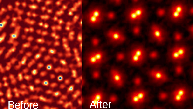
Ptychography works by scanning material in different overlapping areas and measuring the reflected pattern. By comparing the reflections from overlapping areas, an algorithm can reconstruct what the structure was that created the pattern. The team’s leader, [David Muller], likens it to the speckles laser pointer pet toys make. Paradoxically, the electron beam is slightly defocused to capture more data. After data processing, the resolution is down to a picometer.
Currently, the method is time-consuming and requires large computers, but we all know that computers get faster every year, so in a decade your wristwatch will probably be able to do the number-crunching required. The actual paper is paywalled, but if you have access to the kind of equipment you need to do this, you probably also have access to Science or won’t mind spending a little coin to read the paper. If half of the current resolution is sufficient, you might like reading the older paper, too.


Well, I’m glad we got that resolved. 😆
I think the title is supposed to say “Resolution”, rather than “Revolution”. Otherwise very good article.
As soon as I posted my last, the title was corrected… ;)
Always wondered what atoms were going to overthrow?
Oh, that one’s old news. Like 13,81 billion years old. That’s when matter (and therefor atoms) overthrown antimatter. (I heard it was a fierce battle with both sides annihilating the other on contact. Still a mystery how one side managed to do it in the first place with both sides seemingly equally strong.) Or wheren’t you refering to the matter-antimatter imbalance?
It’s a resolution revolution.
Al Williams said, “Paradoxically, the electron beam is slightly defocused to capture more data. After data processing, the resolution is down to a picometer.”
Down to a picometer, that’s impressive. For comparison the structures being made in modern semiconductor fabs today are on the order of single-digit nanometers, more than a thousand times larger.
> modern semiconductor fabs today are on the order of single-digit nanometers
False.
TSMC’s “5 nm process” is a marketing term just like “Coke-a-Cola” is, it has no related to the actual dimensions involved.
TSMC’s “5nm process” has a Transistor gate pitch of 48 nm, and a Interconnect pitch 28 nm.
( ref: https://en.wikipedia.org/wiki/5_nm_process or https://en.wikichip.org/wiki/5_nm_lithography_process )
It is brilliant marketing, because of the amount of technical people who are totally fooled expecting “5 nm process” to have some relationship to what is happening on the silicon.
I did not realize that “5nm” was *entirely* a marketing lie.
I’m confused by your analogy though. What about “Coke-a-Cola” is a marketing ploy?
Sorry I typoed the name very badly. Coca-cola is now purely a marketing name. When launched, Coca-Cola’s two key ingredients were cocaine and caffeine, the name directly related to what was inside the product (but for legal reasons since then the formula has changed but the product has the same marketing name, even though it is no longer related to what is inside the product any more).
And from the 1960s to the late 1990s the process node name more or less directly referred to the transistor’s gate length. Which was the minimum feature set on the chip. This was changed to a purely marketing term by the MBA’s in a 1990’s power move which was probably fueled by coke.
The cocaine was derived from the coca leaf. And the caffeine from kola nut (which at the time was also spelled “cola nut”).
So originally there was a direct relationship between the marketing name and what was inside the product.
I knew all that, but I don’t really see a useful comparison between, “its name derives from something that’s no longer used” and “its name was a complete lie from the beginning.”
One is a side effect of change, one is intentionally misleading.
And if I’m not mistaken, Coca-Cola still does use Coca leaf and Kola nut byproducts in their recipe.
@Jace
Ford is a brand name.
Gucci is a brand name.
Coca-Cola is a brand name.
Intel 7nm process is a brand name. (expected to be) ~237.18 MTr/mm2
TSMC 5nm process is a brand name. (expected to be) ~171.3 MTr/mm2
Intel 10 nm process is a brand name. ~100.76MTr/mm2
TSMC 7nm process is a brand name. ~91.2MTr/mm2
MTr/mm2 is mega-transistor per squared millimetre
(ref: https://en.wikichip.org/wiki/5_nm_lithography_process )
From a marketing standpoint it is genius, totally fools people. Basically from a legal standpoint there does not need to be any relationship between a brand name and what the actual product is, that should be taken care of by the customer, before they buy with their common sense and due diligence.
@Truth said: “TSMC’s “5nm process” has a Transistor gate pitch of 48 nm, and a Interconnect pitch 28 nm.”
Good point. But as I understand it the resolution of the individual edges and/or corners that make up a structure are on the order of 5nm (or so).
‘The term “5 nm” is simply a commercial name for a generation of a certain size and its technology, and does not represent any geometry of the transistor.’ ( ref: https://en.wikichip.org/wiki/5_nm_lithography_process )
When I last worked with cristalography we were working with 1.4 nm. Color me impressed.
“The actual paper is paywalled, but if you have access to the kind of equipment you need to do this, you probably also have access to Science…” Or just go to Sci-Hub.
I’d much rather the people who write and review the papers deposit it themselves. The whole debate that surrounds it would go away. Plus everyone with a clear conscious can say I already paid for that. *
*Even if it’s a paper from another country.
Al Williams said, “The actual paper is paywalled, but if you have access to the kind of equipment you need to do this, you probably also have access to Science or won’t mind spending a little coin to read the paper.”
I say, “The actual paper is paywalled, but if you are smart enough to actually understand the paper you probably also know how to use the great equalizer, Sci-Hub.”
BTW here’s the DOI: 10.1126/science.abg2533
https://arxiv.org/ftp/arxiv/papers/2101/2101.00465.pdf
But why is it red? Also is that H2O?
My guess would be, that they ran out of green electrons, that why it’s red =P
And it seems to be praseodymium orthoscandate (PrScO3) according to the paper.
From the linked article: “a praseodymium orthoscandate (PrScO3) crystal, zoomed in 100 million times”.
Electron microscopes are grayscale, they probably colored it red for visibility (like night vision green) or grabbing attention.
Now we need a small pair of tweezers so we can move them about to make what we want.
IBM has been doing that for years:
https://www.youtube.com/watch?v=oSCX78-8-q0
… And arrange the molecules to spell “Cornell.” (Remember the first time this was done, the researchers arranged the atoms to spell IBM?)
I worked at Cornell a long time ago. Two funny stories. One was a splash screen on a piece of software that I wrote that did not come out as panned. I thought the Sun logo was cool so I tried doing something similar with C and U. I forgot how I laid them out but when it tiled them it made a pretty good Swastika. Oops. The other was our group was one of the first with a big Win NT rollout and I had majordomo set up and had a few lists on it already so I set up a list for Cornell university NT users. I can not believe I did not see it but yea, i had a list called CUNT users til someone pointed it out to me. Oops. We did have some fun back in the day..
“CU See Me” has to be the most contrived ever.
— edw5@cornell.edu
If you want to play with this yourself, for dirt cheap, here’s a non-paywalled similar thing: https://www.nature.com/articles/s41598-019-43845-9
It’s optical, not electron microscopy, but the same principle. Uses a rasp pi + camera. Code & 3D-printable design is available for download.
That is brilliant
Fourier Ptychography algorithm is described in: http://dx.doi.org/10.1364/BOE.5.002376
And there are a few open source implementations of it https://github.com/search?o=desc&q=ptychography
So when an LED’s array is used the sample is stationary, and an image is captured when each individual red,green,blue LED in the array is turned on. So a 16×16 RGB LED array would typically generate 256 x 3 images. And these images would then be processed using the Fourier Ptychography algorithm to calculate the high resolution image.
And in the above example there is only one electron beam in an electron microscope so the sample is physically moved multiple times instead to generate the multiple images to calculate and compensate for all the distortions in the system.
What would be interesting to see, would be the resolution possible if a 1920×1080 RGB LED array was used. But the exposure time for such an array and the processing time (around 6 million images) would be totally insane.
After watching this: https://www.youtube.com/watch?v=ULZtv31it60
I wonder if you used a grid of 16×16 HD image sensors, could you record a video and after the fact adjust what is in focus using the same computational technique.