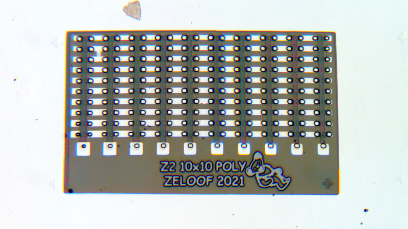
Back in 2018 we reported on the first silicon integrated circuit to be produced in a homemade chip fab. It was the work of [Sam Zeloof], and his Z1 chip was a modest six-transistor amplifier. Not one to rest on his laurels, he’s back with another chip, this time the Z2 is a hundred-transistor array. The Z2 occupies about a quarter of the area of the previous chip and uses a 10µm polysilicon gate process as opposed to the Z1’s metal gates. It won’t solve the global chip shortage, but this is a major step forward for anyone interested in building their own semiconductors.
The transistors themselves are FETs, and [Sam] is pleased with their consistency and characteristics. He’s not measured his yield on all samples, but of the twelve chips made he says he has one fully functional chip and a few others with at least 80% functionality. The surprise is that his process is less complex than one might expect, which he attributes to careful selection of a wafer pre-treated with the appropriate oxide layer.
You can see more about the Z2 in the video below the break. Meanwhile, should you wish to learn more about the Z1 you can see [Sam’s] Hackaday Superconference talk on the subject. We’re looking forward to the Z3 when it eventually arrives, with bated breath!


More than 16 times more transistors every three years. We’ll be buying CPU’s from him in 15 years (hoping on a more than linear expansion)
Moore’s Law can get rekt
Moore’s Law can go get rekt, Zeloof’s law’s where it’s at
If there’s an apocalypse we know who’s going to be part of restarting civilization.
He could literally make a 555
If you’re in need of a 555, just go through the comments here. Theres plenty.
I actually can’t help myself – for others that may stare at this comment for a few minutes wondering what the in-joke is…. a 555 is…. an old timer.
well played, sir.
555 is an old timer…..this old timer took a few minutes to grok that. Nice!
Well, its true.. and alt easier to.. of you can handle the old time(r)s.
Think he’s referring to people constantly saying stuff like ‘you could have done that with a 555 timer instead of using a full blown microcontroller/raspberry pie’. I like your interpretation better tho
Blinking LED with a quad core, 4GB Raspberry Pi :P
Then he could make a 3909 LED flasher, which is no longer made. For some uses, better than a 555.
In 1976, I was given atube of 555s. I still have some. I guess a syatement on how I reuse parts, rather than a dismissal of tIe 555
That’s amazing.
I still think they should have called it “the fine art of making teeny tiny things” instead of “microfabrication” but that’s just me.
Very impressive result! Perhaps the Z3 design could be a MC14500 clone? :-)
Or simply a Y8
it’s the pure 8-bit RISC core I develop at https://hackaday.io/project/27280-ygrec8
It would be easy to map to NANDs and NORs, so Sam just has to design an appropriate “gates library” and the Y8 would probably map 1 to 1.
I see a convergence here ;-)
or a CEM3381 dual VCA chip on a 8 pin dip. Quite unobtainium. Not a big deal to replicate.
Right now he made some N-type MOSFET. The only type of logic he could be making is NMOS.
At some point, he’ll need to be able to make PMOS transistors to make CMOS (as in complementary i.e. P + N transistors). Making PMOS transistors on top of the P well would mean at least 2X the number of steps.
Circuit complexity would need some routing layers. Think of it as routing a PCB, how many time you would need to add jumpers or go beyond a single layer for anything non-trivial?
Don’t hold your breath.
Don’t forget his z1 chip used PMOS transistors. NMOS ICs are apparently harder to do and suspect it may now even be possible for him to make an original 6502 CPU (which uses NMOS).
Going to CMOS is one of his stated future aims in his current blog, so I’ll keep watching this space :-)
Intergrated circuit ?
Intergated ? :-)
Apparantly…..
Halfway between grated and not grated
Right now it is more like a transistor array than anything else. :P
This is sooooooooooooo cool! Wow!
I wonder, if a plan is to do the layout for a small Gate Array.
I assume many people would have a suggestion for a functionality to try it out.
Nice. Obviously i don’t have the same stuff in my garage as this guy.
I put off watching this vid until I had more time, and now I’ve seen it, all I can say is wow!
This guy *might* have a lot of time and money, but that’s probably not true. I know a guy that has a mass spectrometer in his garage and works for a pretty measly salary. I’d take a wager he got most of his gear on the cheap by knowing people in the know and being at the right place at the right time.
Start collecting! You’d be surprised what you can find as surplus.
So this is the guy who will help solving the chip shortage?
Amazing work, like small companies launching rockets into space where in the 60s it took a nation state, one dedicated individual is doing now what it took thousands of engineers to do back then. Thanks for sharing this alchemy with the world, demystifying this process.