We were trading stories of our first self-made PCBs in the secret underground Hackaday bunker, and a couple of the boards looked really good for first efforts. Of course there were mistakes and sub-optimal routing, but who among us never connects up the wrong signals or uses a bad footprint? What lead me to have a hacker “kids these days have it so easy” moment was that all of the boards were, of course, professionally fabbed with nice silkscreens. They all looked great.
What a glorious time to be starting down the hardware path! When I made my first PCB, the options were basically laying down tape, pulling out the etch resist pen, or paying a bazillion inflation-adjusted dollars for a rapid prototype board. This meant that the aspiring hacker also had to have a steady hand and be at least casually acquainted with a little chemistry. The ability to just send your files out to a PCB house means that the barrier to stepping up your hardware game from plug-them-together modules is lower than it’s ever been.
But if scratching or etching your own PCB out of copper plate is very hands-on, very DIY, and very low-tech, it’s also very fast in comparison to even the most rushed service. Last weekend, I needed a breakout board for some eight-pin SOIC H-bridge chips for a turtle robot project with my son. Everything was hand-soldered and hot-glued in a Saturday afternoon and evening, so there was no time for a PCB order. A perfect opportunity for the Old Ways™.
 We broke out a Sharpie, traced out where the SOIC pins would land, connected up the grounds, brought the signals out to friendly pads, and then covered the rest of the board in islands of copper just in case we’d need any prototyping space later. Of course, some of the ink lines touched each other where they shouldn’t, but before the copper meets the etchant it’s easy enough to scrape the spaces clear with a pin. The results? My boards look like they were chiseled out by a caveman, but they worked. And more importantly, we got it done within the attention span of a second grader without firing up a computer.
So revel in your cheap offshore PCB factories, hackers of today! It’s a miracle that even four-layer boards come back within a week without breaking the bank. But I encourage you all to try it out by hand as well. For large enough packages and one-offs, full DIY absolutely has the speed advantage, but there’s also a certain wabi sabi to the hand-drawn board. Like brush strokes in residual copper.


I have to say I am yet to outsource my projects to a foreign board house. The last tome I used a board house it was a couple of weeks and I could just drive across town to pick them up. And yes it was the bazillion dollars a board.
But still today I etch my boards in the garage and am currently working on having a go at milling them – with the challenge that is throwing up i think etching is a simpler process
But DYI is not about simplicity. Otherwise you might stop with this hobby right now. So go on and build your own CNC to mill PCBs. :-)
For one-offs you can get more creative than regular printed/etched boards too. How about a glass board with real copper wires glued to it? Why even stick to a flat board, when you can use a cube, cylinder, ball, or any shape you like? DIY is *MUCH* more fun than sending it to an offshore manufacturer. If you’re going to copy mass produced products, you might as well buy the mass produced product.
https://www.youtube.com/watch?v=Rnbfre4xATQ use a laser? even the wimpy 2W ones will do.
The secret layer isn’t floating in the sky?
They first circuit board I bought was phenolic? Smelled bad, and shattered easily when I tried to cut it. And once etched, the traces would come off so easily. But 99cents for a pretty large sheet, and I could get it at the store downtown.
I made some boards that way, but nothing serious. I think I used a laundry marking pen that was around to lay out resist. Very crude, not only were the resulting traces uneven, but no attempt at straight lines.
It got better with better board, but also I got access to drafting tape. Lay it down on the board, and etch.
Much later I tried with a Sharpie, very fast. I seem to recall it becoming known that the resist pen in the Radio Shack etching kit was an unmarked Sharpie.
What I really liked was the Letraset like rub on traces that Radio Shack (and surely elsewhere) sold. That was easier to lay down than drafting tape, but neater than a Sharpie.
The hardware store sold the needed tiny drillbits. They’d put them in a big manilla envelope to take to the cash, and the cashier woukd open it, and not find the tiny drillbits hidden in the bottom.
Early on, I got a drill press adapter for my electric drill, less breakage of drillbits after that.
I’d clean the boards by putting some of that plastic “steel wool” on a sanding disk, really shiny copper after that. And then I’d spray the finished boards with clear Krylon.
Either I bought a photo etching kit, or someone else did. But for some reason, we never tried it.
I got a book about amateur radio projects that came with layouts for all the projects, I think in some other paper that you were supposed to remove. It was still in print in the seventies, but from earlier. Something that arrived in hobby circles at a finite time, and for a bit, the circuit board was primary rather than the circuit. I think there were some projects in Elementary Electronics where you could send fifty cents and get the circuit board. So for a while, construction articles would spend time explaining how to make circuit boards.
I have used a Dremel tool to carve a blank circuit board. Fast, but messy.
My first attempts at making my own PCB’s was in the 70’s, with the stuff available a Radio Shack. That etchant was some NASTY stuff… it stained ANYTHING it touched, including your skin. Get a drop on your clothing? It was PERMANENT. ;) I made a small handful of boards in my teens, and soon just gave it up. Been using vectorboard ever since! :) My favorite is the kind that resembles the plug-in breadboards. Lots of flexibility, and I’ve built some fairly complex circuits on it over the years. :) I have also done the Dremel tool method for simpler circuits, where you can easily get by with a few larger pads and such. You’re right… MESSY! But it still beats that awful etchant! ;) I have a project I’m thinking about getting some fabbed boards, tho… been mulling that one in my head a while. Some places it’s $51 for 3 boards… but that was a couple years ago. Have prices come down THAT MUCH since?
OSHPark is $5/sq-in for 3 2-sided boards shipped in about 10 days. It’s my default fab now.
+1 By the time you pay expedited shipping from China, It is not much cheaper. So my boards are purple.
These days I think the laser print toner transfer method is the obvious choice for quick and dirty. Certainly what I will be using, at least until I CNC my mill or build a better one for it, whenever I can get the parts I need for the few simple projects I’ve got in mind…
I don’t mind sending out to fab houses, but you actually have to pay attention to so many details to meet their criteria for the price bracket you want, wait for shipping – what is the point for simple easy to one side projects… When you actually need to put that much effort in for your more complex project great, but when as you so ably demonstrated hand scribbled permanent markers will do…
I wanna see the secret bunker! Pictures, drawings, build log, everything!
It’s like inside the cover of Tom Swift Jr books
Exactly how _secret_ would it be if we published all that documentation?
Hey, I’m not asking for the location..
My thought too.
Batman had visitors to his Batcave, but he used Bat Knockout Spray sothey wouldn’t know how to get there.
Funny enough, during our regular hack-the-space day at our makerspace, just this morning I dug out some PCB footprint and track transfer sheets, of the kind I talked about (in the super secret bunker) using as a kid. I’ve rescued them. I may make a little board with them direct onto clad board, just for old times’ sake.
I found my Mum’s nail polish was good for thick traces and filled areas, saving my etch resist pen. And if I filled as much of the board as possible, saved my echant too. But somehow she was not impressed by my creativity.
My mom was not impressed when she found out that I was using her food coloring to refill my fountain pen cartridges.
This was fun back in the day but while reading this my inner second grader (never far from the surface) waved his hand and asked “why not play connect the dots with a solderable breadboard?” After RS’s demise, I’m a lot more likely to have “blanks” of those around than ageing bottles of etchant.
I do the same thing. :) My favorites are the ones with the pattern similar to the solderless breadboards. They make them in all kinds of sizes, now, which is great! I buy mine from http://www.mpja.com which is an AWESOME source for tinkerers!
Man, yes, the days.
In the late 80’s it was expensive to do a run, and working in a small company I etched and drilled many a boards. I got kinda good at it.
Initially I hand rendered the layout in pencil and then inked the final, taking it then to a photographer for reduction to ortholiths. This was actually cheap and quick. Like ten dollars and sometimes would be turned around while I waited. The traditional pre-press business was collapsing at the time due to the advent of ‘desktop publishing’ as we called it then, so they were happy for my business, weird though they thought it was. Later I got a better plotter and just did the photog myself with Kodalith. It was surprisingly easy.
I did two-sided boards by making a sandwich of the front and back litho aligned and commited with Scotch tape, and then sliding in the sensitized board. The boards would be scoured with Comet, and then sensitized with KPR. (I still have half a quart — it lasted forever. Good luck on finding developer, though!) Expose under a sunlamp bulb (UV-B) and you were good.
I initially used FeCl but eventually preferred Ammonium Persulphate because I could see what’s happening and so I could get fine lines reliably.
I never mastered plating. Instead I tried to minimize vias (which I just soldered a wire through pre-population with components), and then used the leads of the through-hole components to provide the rest of the layer transitions.
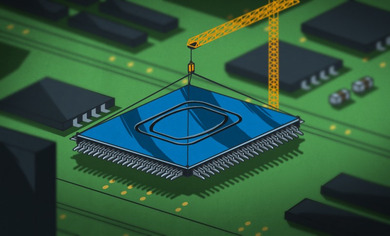
Now is a new day. Now we can get boards made with four layers, through-plating, solder masks, silk screens, for mere tens of dollars.
We live in a truly glourious time.
the biggest reason i’ve never homemade boards is that i don’t want to get in the business of storing or disposing of etchant and etchant-waste. what do you all do, practically speaking? do you just have one batch of “Copper Chloride in Aqueous Hydrochloric Acid Solution!” that you keep forever, or do you make regular trips to your county’s hazardous waste disposal facility?
The stuff can be neutralized and correctly disposed, at a convenient time. Or just do like those “overseas board houses” do, and dump it into some river.
Or do the sensible thing and use a decent bottle to store it in for later – blow some more air through it and its good to go again (at least with the right etchant). And for your normal sized DIY boards you really don’t need to store that much of it..
If you are using FeCl3 or HCl and your wastewater goes to a sewage treatment plant, neutralize with NaOH and flush it down the loo. Only the copper ions are problematic, but in the sewer your brew will thinned down to a homeopathic level – well below the amount of copper that permanently leaks from plumbing and roofs.
Of course it is better to not dissolve copper with etchant in the first place, so use wide traces and the “copper pour/fill” function of your PCB software. If you design for minimum spacing, you can etch several m² with 1kg FeCl3.
Re: one batch of etchant. Yup.
In the last 15-20 years, I have been to the toxic waste disposal exactly once for etchant, and that was because I moved to Germany and didn’t want the hassle of shipping it. I also made up a batch at my old hackerspace, and I probably should have disposed of that before I left — sorry y’all!
Shortly after arriving here (10 years ago now!) I ordered up some peroxide and hydrochloric on the internet and made up about 300 ml, and it’s still about 300 ml, just an ever-darker shade of green.
I guess that some copper leaves the system via the few drops you rinse off the board or out of the funnel. Sometimes I squirt in a little more peroxide. It hasn’t seen more acid in ages, and I haven’t tried to figure out the pH because it just works. But you could.
Secrets include:
1) Etch in tupperware, b/c you can seal it which prevents both fuming and spills, which are basically the two hazards.
2) Store in an airtight plastic container — a PETG soda bottle is perfect. Fumes and spills again.
3) Keep the sink full of water, b/c you _will_ spill a drop or two, and you don’t want to etch the sink stopper. It’s neutralized essentially instantly when diluted, at least with our hard water. (Green to blue is the telltale.)
4) As long as you’ve got tupperware and a sink full of water, you might as well float the thing in warm water to speed the reaction along.
5) Agitation. Constant. Until it’s done. It’s only like 7 minutes.
6) Designing boards for minimal copper removal speeds things along. As you etch, the etchant will get darker and slower. The less copper you need to remove at once, the less etchant you need to keep on hand to get the job done. I literally have ~300 ml of etchant, and I pour the whole amount into the tupper every time, b/c why not? If I need to etch enough copper off that it starts to darken/slow, I’ll toss in a capful of peroxide, and that perks it right back up. Oxygen is the limiting reagent.
So… storing you have to do, but disposal is a rather infrequent occurrence. If it gets brown, add peroxide. If it gets too slow, add acid. (But if you keep the acid from fuming off in the first place, you won’t need to do that often.)
On the topic of acid, air regeneration is, in my experience, a waste of time. You don’t want it fuming, so minimizing air contact is a good idea. (Fuming means the solution gets less acidic, but also that metal in your bathroom rusts. Ask me how I know.) Capful of peroxide solves the problem much easier on hobbyist scales. If you’re running industrial production, it might be cheaper to somehow bubble up air through the solution. None for me, thanks.
I’m using FeCl3 at maximum strength (density about 1.4 kg/l, the Bungard stuff Conrad sells). Etching is done in a transparent Lock&Lock food container which can be held against a lamp to see if it’s finished. It takes <3 minutes with agitation at room temperature when the etchant is fresh, now after at least 50 eurocards the brew has turned a bit greenish and needs some heating. I'm storing the stuff in a detergent bottle with a wide opening, which can take an aquarium heater for heating to 40°C.
I've tried HCl+H2O2 a long time ago, but was not amused about the fumes and the availability of the two components. Sourcing reasonably strong HCl and H2O2 is somewhat difficult nowadays.
I tried to make my own PCB back in the 80s. What stumped me was not so much the etching but the drilling. I found it impossible to drill a DIP14 pattern even with a drill press. And, of course, no through-plating, no mask or silkscreen, and I didn’t even try to line up double sides.
Yeah, manually drilling PCBs was no fun 40 years ago and presbyopia didn’t make it easier. Recently I replaced the Proxxon drill press with a cheap CNC toy, probably my best investment in tools ever.
Regarding double sided PCBs: use one side as an exclusive ground layer, without etching. Chamfer the holes that have no ground connection, solder grounded component leads on both sides. You may also use tiny copper rivets (availabe at the usual chinese sources) as vias.
Drilling sucks. SMT rocks. Problem solved?
I’d love the excuse to set up a drill-file-to-gcode toolpath for my CNC router to drill the holes for me, but I honestly have avoided drilling more than 16 holes on any given board in the year since I got the CNC, so it just hasn’t been worth it. Some day.
I mostly use prefboard, wire wrap and point to point. I’ve had boards made by pcbway and they were fine but I only need one board 99 percent of the time.
Back when radio shack was going bye bye the second time I bought some etcher and copper clad boards but never used it. I am half tempted to build a little CNC and try milling out a pcb.
i’ve mostly given up on etching. they look pretty, but when the board is buried into the project anyways, it’s wasted effort.
for the most part, i’ll design the board as i normally do, then print it out to scale on normal paper. tape that paper to a piece of FR4, and then just use a dremel and cutoff wheel to separate the copper layer to the required design.
it’s quick, easy, and works just as well as a fully etched board. the side benefit is that for the thermal-dissipation of certain components, i gain a little more surface area than i normally would with etching, as any ‘trace’ is now just any amount of unused space between points.
Totally. I do that too — cut out copper with a knife instead of a dremel — but when there are more than ~10 lines, or they’re really close, I’ll let teh chemicals do the cutting.
For RF, just build over the unetched circuit board. Not so neat, but easy to change, and always a good ground. Less easy for DIP ICs.
There were tools in the past for cutting “pads” in the circuit board. Carving with a Dremel is sort of like that, except areas carved out, not pads. I remember one article in the seventies suggesting a hacksaw across both vertical and horizontal, so you have a grid of squares insulated from each other.
A long time ago, there were insulated pins, drill a hole and insert. A variety of kinds, the only ones I had came from prototypes
Some people glue pads onto a larger sheet of copper circuit board. I suppose neater than just hanging off leads, but seems too much effort. And somehow that turns into some people buying pads, litle squares of circuit board. Might as well just use scraps you have.
My first home made boards were not all that long ago, maybe late 2000s. I did laser printer toner transfer, I had this glossy xerox laser photo paper, used an iron to transfer and soaked the board+paper in water until the paper fell off. To etch I used muriatic acid and hydrogen peroxide. Worked really well, I had no problem doing smaller SMT ICs. The waste solution I would neutralize with baking soda, then absorb the liquid into oil absorbant granuals for later proper disposal.
Those were the days. Then Ian Lesnet started DirtyPCBs and I never made my own board again.
It’s easy enough with home equipment and the right methods. Namely ‘drafting film’ for artwork print, laser printer, print two copies of the artwork and overlay them to get rid of the ‘holes’ in the laser print.
Use a ‘ground fill’ in your CAD to reduce copper removed.
Etch in a homemade bubble tank with Ferric Chloride and it’s fast and will last years for a hobbyist.
I could easily get 10 Mil tracks with this method. Here is an board I made in 1999.
https://mecrisp-stellaris-folkdoc.sourceforge.io/pcb.html?highlight=pcb#hand-etched-single-sided-microcontroller-board
CAD was gEDA; gSchem for the schematic and PCB for the board layout.
I started this year with diy circuit boards. The etching and the toner transfer is easy enough, but i seriously underestimated the amount of work it is to draw the circuit, select the right component footprints, and then route the whole thing properly (or to select the right locations for the components when auto routing).
In the end, for prototyping using a universal prototyping board or some stripboard is still the fastest way to get something done.
still haven’t tried the chinese pcb fab houses yet. i don’t like change. especially since i got a massive pile of pcb stock that i want to use up first.