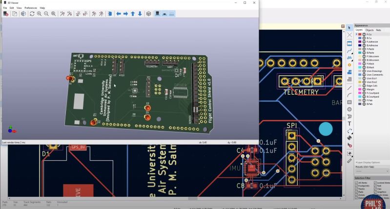
In a recent retrospective video, [Phil] from Phil’s Lab goes through a number of his early PCB designs, to critique and comment on what he likes and doesn’t like in these designs. Even though it’s only been a few a few years, he founds plenty that’s wrong. From poor and inconsistent formatting in the schematic, to sloppy and outright broken PCB layouts. It’s a fascinating look at years of lessons learned.
[Phil] comments on the importance of clear labeling and organization of sections and pages in the schematic to make it obvious what the function of a block is. Other lessons include the labeling of nets to make PCB routing a lot easier, making good use of PCB planes, getting all relevant information on components and layout in the schematic as a comment, and connecting decoupling capacitors to their relevant pins.
Although we tend to forget about older projects, it can be very interesting to take a look at them now and then, to see (hopefully) our progress over the years. In the case of [Phil] it’s fascinating to see the transition from a basic two-sided board with THT components to multi-layer boards with STM32 MCUs.


Also, examining others’ PCB designs for interesting approaches to doing things, or asking “why is this done this way?”
I especially like to look at really aesthetically pleasing, clean circuit boards. Most of the time my boards are getting uglier, the more space I try to save…
Thanks for writing a Hackaday article about the video, Maya! Let’s see what the next few years bring w.r.t. PCB designs and improving skills :)
Phil
Impressive progression of skill in a short time.
My own #1 lesson learned: Add test points. Or more generally: Design for test.
And a hint: If test points are made with large vias, then use an extra dummy board, install pogo pins in those vias, and these exactly match the board under test. Easy bed ‘o nails.
Schematics or logic diagrams have to flow or the boards will likely end up looking like the schematic, a hodgepodge of
of disassociated parts wherever they fit. Boards have rules, material, size, power/ground planes, I/O locations, skylineing with other components etc.
Oh, that hint is great, gotta find a use for those extra boards in the qty5 order. I’ll make use of that, thanks!
I’ve been using pogo pins for test and programming fixtures for ages, but the dummy-board trick I shamelessly stole from Hans Summers (qrp-labs.com). See his explanation and more helpful hints here: https://youtu.be/xb_ZmPx7Py4?t=628
Start at the beginning of the video for the backstory.
Okay- This is genius! I’ve always just been careful to keep test points on a grid and use protoboard (through hole test points are far superior. how the hell am i supposed to hold my probes on a flat pad?), but this is so much more flexible- and, like the other guy said, a good use for those excess boards. defo stealing :)