The Ball Grid Array, or BGA package is no longer the exclusive preserve of large, complex chips on computer motherboards: today even simple microcontrollers are available with those little solder balls. Still, many hobbyists prefer to stay with QFP and QFN packages because they’re easier to solder. While that is a fair point, BGA packages can offer significant space savings, and are sometimes the only choice: with the ongoing chip shortage, some other package versions might simply be unavailable. Even soldering doesn’t have to be complicated: if you’re already comfortable with solder paste and reflow profiles, adding a BGA or two into the mix is pretty easy.
In this article we’ll show that working with BGA chips is not as difficult as it may seem. The focus will be on printed circuit board design: how to draw proper footprints, how to route lots of signals and what capabilities your PCB manufacturer should have. We’ll cover soldering and rework techniques in a future article, but first let’s take a look at why BGAs are used at all.
What’s All This Ball-Grid Stuff, Anyhow?
As computer technology advanced in the 1990s, the motherboards inside our PCs became more and more complex. The 8-bit data buses from the 1980s gave way to 16-bit, 32-bit and even 64-bit wide buses between the CPU, the main memory and expansion cards like hard disk controllers and display adapters. These buses all had to be carried into and out of various chips, which therefore needed lots of pins.
The typical package for complex chips at the time was the quad-flat-package (QFP), with long rows of gull-wing shaped pins on each side. When scaled up to a pin count of 200 or more, these packages became increasingly unwieldy: not only did they become very large compared to the chip inside, the pins also became extremely small and fragile. Large QFP chips required careful handling to avoid bending any pins and making the chip unsolderable.
The Ball Grid Array package, or BGA, was developed to solve both of these problems. Placing the pins in a grid at the bottom of the package, instead of spreading them around the edge, makes for a far more area-efficient design. In addition, solder balls are much more robust than the tiny little pins on small-pitch QFP packages. Although manufacturers initially feared manufacturing and testing issues, the BGA package turned out to be very reliable and has since become ubiquitous in all types of electronic equipment.
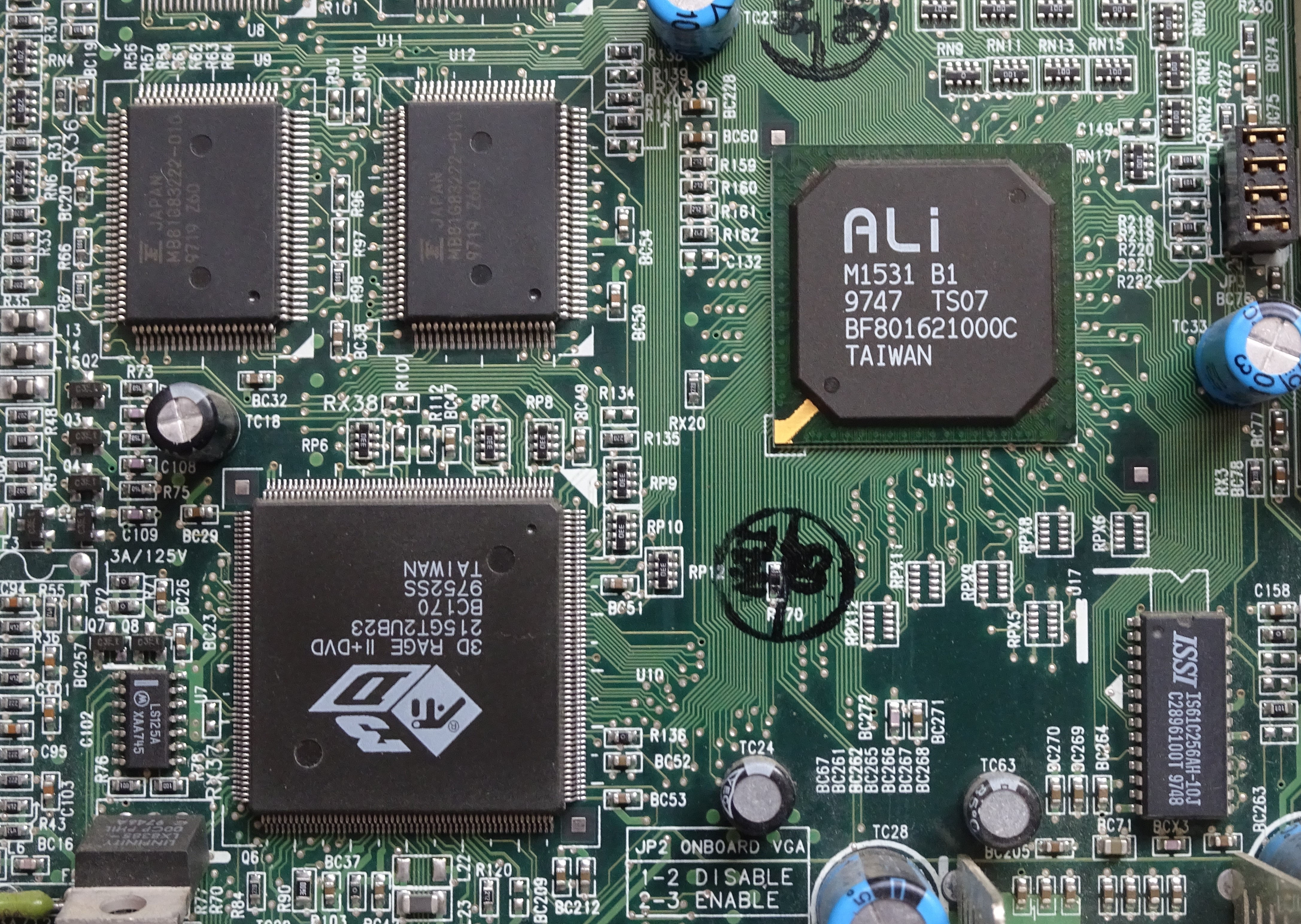
The picture below, showing part of a 1997 vintage PC motherboard, clearly illustrates the difference in area efficiency between a QFP and a BGA package. The ATI VGA controller on the left has a 208 pin QFP package with a 0.5 mm pin pitch. The Ali M1531 system controller, on the right, manages to fit 328 pins on its BGA package, with solder balls at a much more comfortable 1.27 mm pitch.
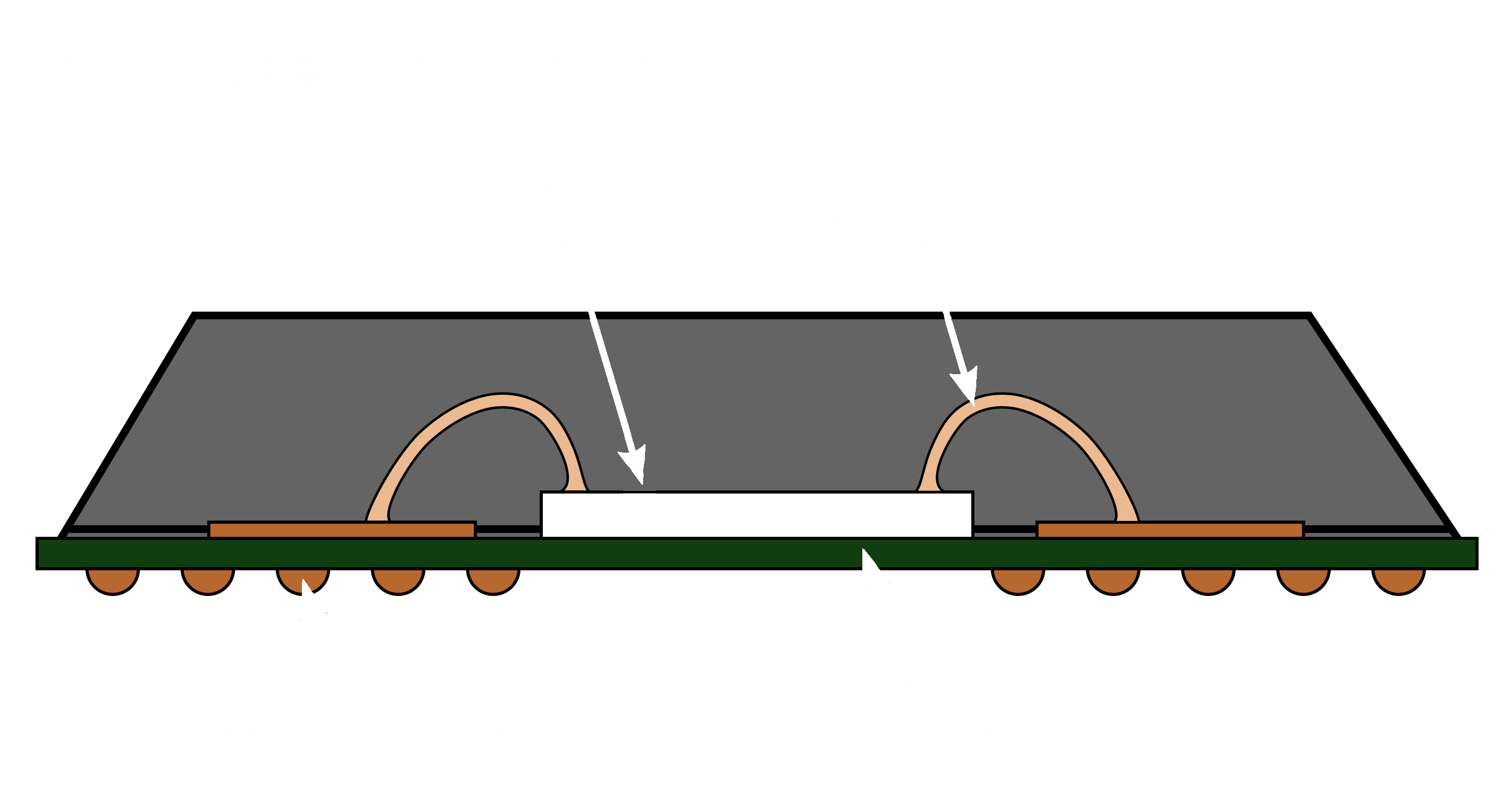
A BGA package is typically built around an interposer: a small printed circuit board that serves as an interface between the actual chip and the circuit board onto which it is mounted. The chip is wire-bonded to the interposer and covered in protective epoxy. The interposer routes the signals from the edge of the chip to an array of pads on the bottom, onto which little balls of solder are attached. The completed BGA package is then placed onto the printed circuit board and heated. The solder balls melt and create a connection between the board and the interposer.
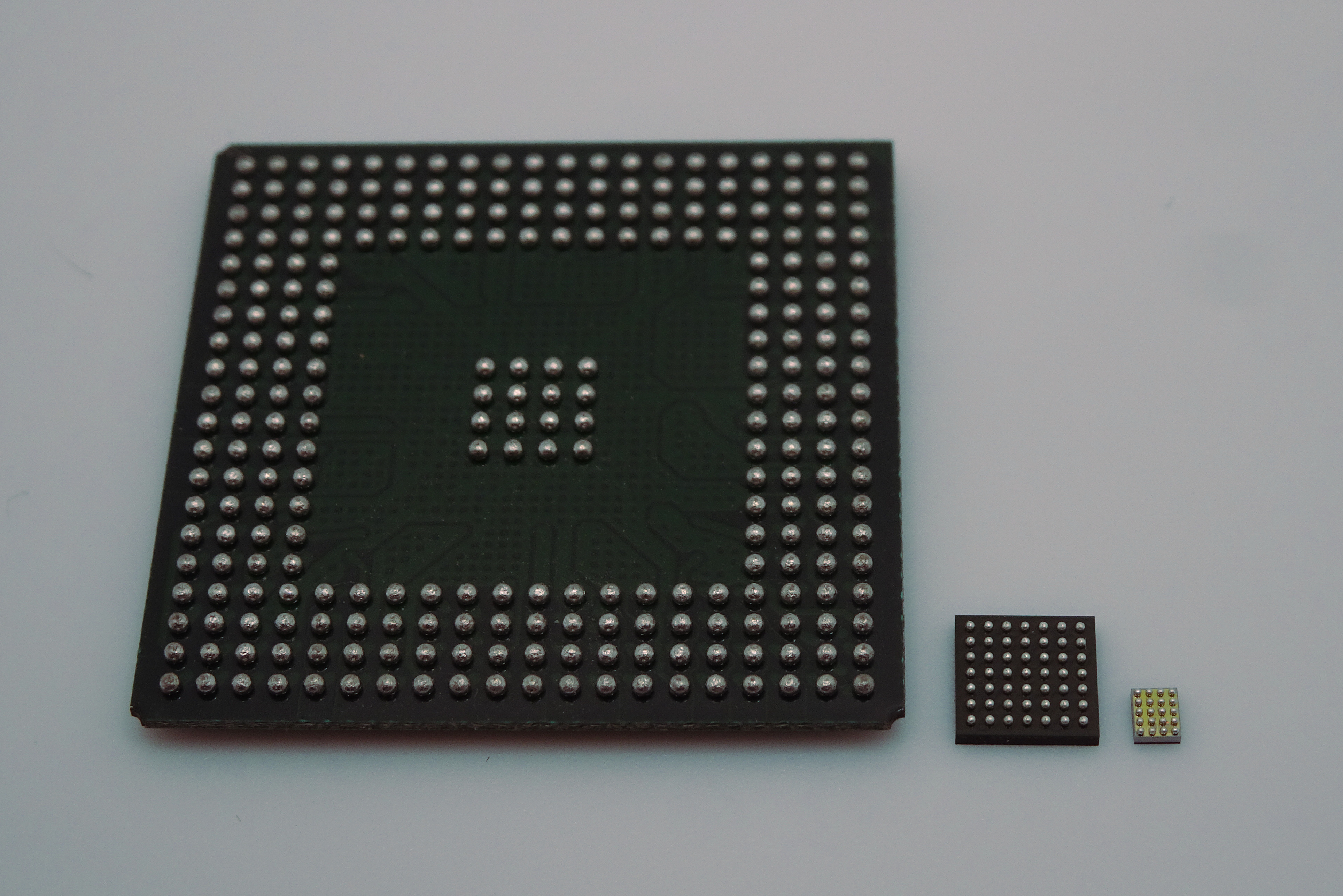
Typical BGAs in the early days had a ball pitch of 1.27 mm. As technology improved, BGA packages became smaller and smaller, until the interposer was not much larger than the chip inside. These miniaturized BGAs are known as chip-scale packages, or CSPs, and typically have a ball pitch between 1.0 and 0.5 mm.
The quest for miniaturization did not end there however: semiconductor manufacturers eventually developed the flip-chip BGA, or wafer-level chip scale package (WL-CSP), that dispensed with the interposer altogether. Instead, flip chip designs place the solder balls directly onto the chip’s surface, with a pitch that can be as small as 0.3 mm. The chip is then mounted upside-down onto the circuit board, either with a protective layer of epoxy on its back or with no packaging at all.
There’s a huge variety of marketing names for different BGA-type packages, with little standardization between manufacturers. But if you simply want to use a BGA chip, it doesn’t really matter what it’s called or even how it was made: the PCB layout techniques are the same for all types. So let’s have a look at how to design PCB layouts for them.
BGA Basics: Pads and Footprints
Picture the following scenario: you’re designing a state-of-the art LIDAR setup, and you’ve chosen TI’s TDC7201 time-to-digital converter to perform time-of-flight measurements. Unlike its predecessor the TDC7200, this chip is only available in a 25-pin nFBGA package, so you have no choice but to make a BGA board. You also need a microcontroller to do some data processing and decide on a Microchip ATmega164. Unfortunately, today’s chip shortage means that the QFP and QFN versions are nowhere to be found, so you end up stuck with the 49-pin VFBGA version. As for the LDO regulator to power the whole thing, you stumble upon a great bargain: your favorite supplier has ONSemi’s NCP161 on sale. As you may have guessed, that one also comes in a BGA package, a tiny four-pin version in this case.
So how do you go about designing a PCB for this trio of BGA chips? As always, the manufacturers’ datasheets are a great place to start. Let’s first have a look at what ON Semiconductor says about how to draw the proper footprint for their NCP161: on page 21 of the datasheet we find the recommended land pattern that specifies a 0.15 mm pad diameter with NSMD type pads.
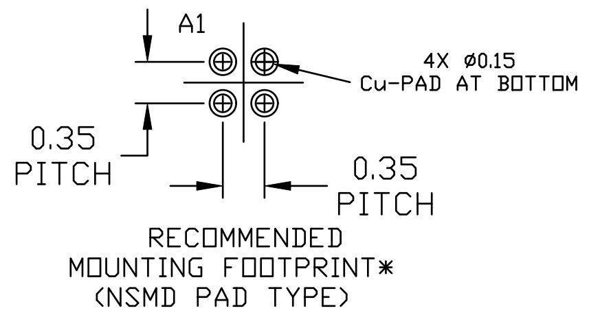
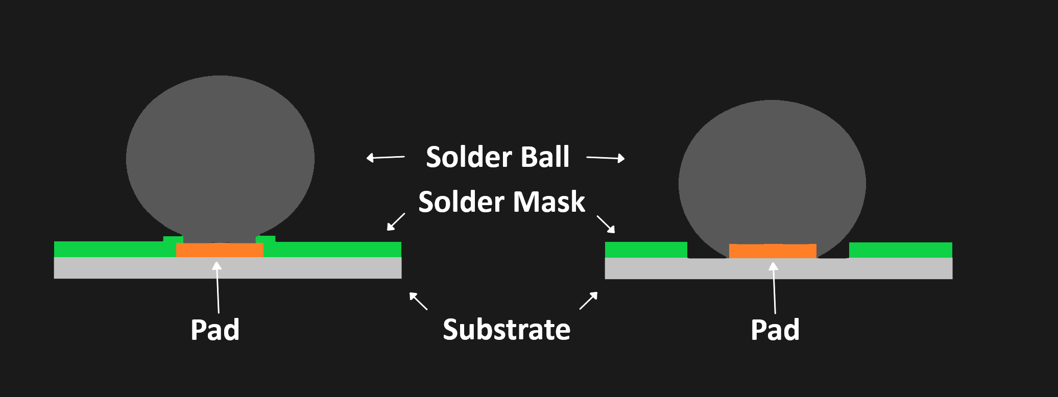
NSMD stands for “Non-Solder Mask Defined”, which refers to a solder pad that is not partially covered by the solder mask. The other option is a Solder Mask Defined pad, in which the solder mask does cover part of the pad. While both types have their applications, the NSMD type is usually recommended in manufacturers’ datasheets for BGA chips because it enables a more robust solder connection: the solder ball can grip the sides of the pad as well as the top.
If we draw a footprint for our little four-pin BGA package in KiCAD, the two options look as follows. The copper pads are shown in red, with the solder mask openings in purple. The pink outline is the component’s courtyard, which determines how close other components may be mounted.
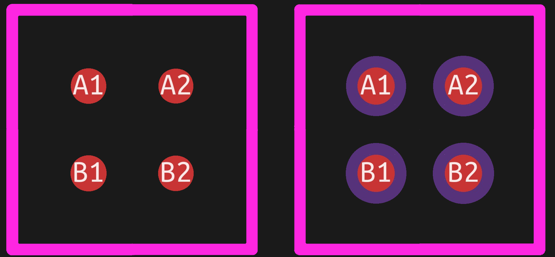
For the NSMD version, the solder mask openings should be slightly larger than the copper pads; in this case, we’ve used 0.25 mm openings on 0.15 mm pads, which means the solder mask openings extend just 0.05 mm on either side of the pad. You should check with your PCB manufacturer if their solder mask alignment is accurate enough to do this; a typical values is 2 mils (0.05 mm), which means that in the worst case, your solder mask will just about touch the edge of your pad. If your manufacturer cannot provide more accurate alignment, you might want to enlarge the solder pad opening a little bit more. Keep in mind that the remaining solder mask between the pads should then still satisfy the minimum solder mask sliver rule.
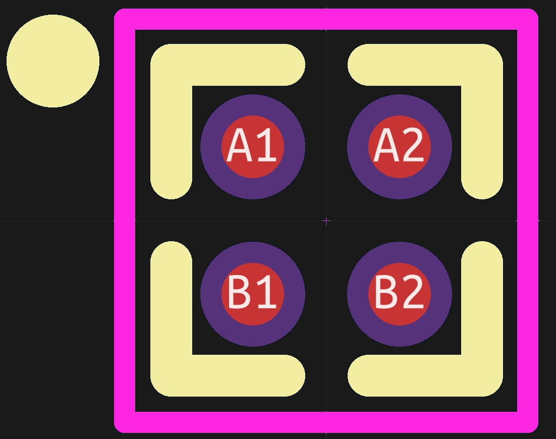
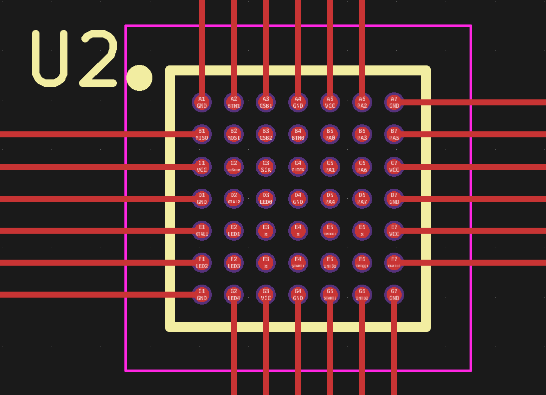
Note that the pads of BGAs are not numbered sequentially, but in a row-column format: the rows are labelled A, B, C and so on from top to bottom, while the columns are numbered from left to right. Pin A1, in the top-left corner, is normally indicated by some mark on the top side of the chip to help you orient the part correctly.
One thing that will be of great help when assembling your PCB, especially if you’re doing it manually, is having the package outline indicated on your silkscreen layer. Since you can’t see the solder balls and the pads when you’re placing the chip, the silkscreen is the only way to tell if you’ve positioned your chip correctly. Don’t forget to draw some sort of indicator to point out which pin is A1, otherwise you’ll still end up guessing which of the four orientations is correct.
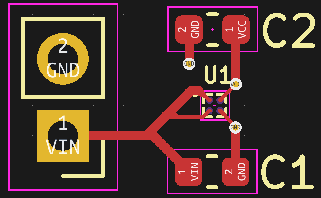
With just four pads, hooking up this voltage regulator chip to the rest of our circuit is easy. While it might be tempting to draw a few big power planes for the input, output and ground connections and overlap them with the pads, it’s usually better to draw a thin trace to each pad first, then connect that trace to any larger structures.
The reason for this is solderability. When the solder ball melts, it will try to adhere to any copper it can see, which means both the solder pad and the trace connecting to it. The chip will therefore experience a slight pull in the direction of the trace during soldering. Making the connections radially symmetric should cancel out the forces exerted by each solder ball and ensure a more predictable soldering process.
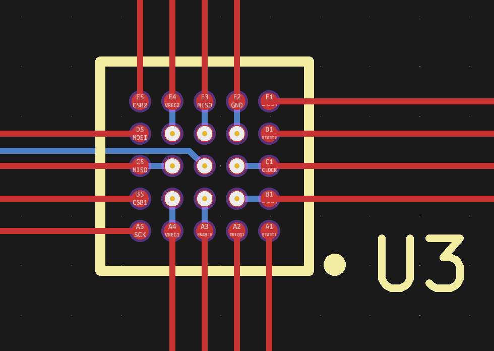
BGA Routing: Dog-Bone Layout
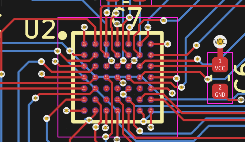
Things get a bit more complicated when we place our microcontroller, with its 7×7 grid of solder balls. Routing traces to all 49 pads is not so straightforward, so let’s start with the easiest bit: the outer pins. We can simply route them outward using horizontal and vertical traces.
The second layer of pins can be routed with tracks going between the outer pads. Of course, our PCB design rules should allow this: the minimum trace width and clearance should be no more than c = (p-d)/3, where p is the pad pitch and d is the pad diameter. For this example, with a 0.65 mm pitch and 0.35 mm diameter, the minimum clearance and track width comes down to 0.1 mm: tight, but still possible at many manufacturers.
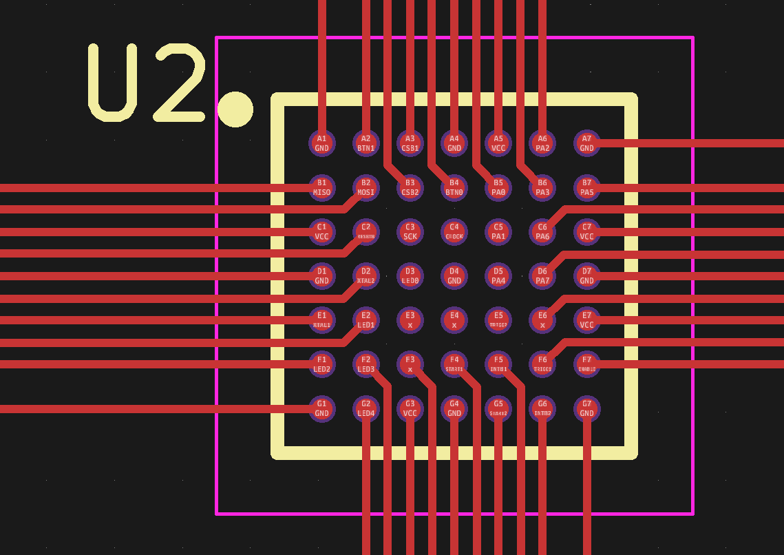
From the third layer inwards it gets more interesting, because from this point on we’ll need vias to get our signals out. The most common way of doing this is to place one via in the middle of every four pads and route a diagonal trace to it from one of the pads.
Of course, we should first make sure that we have enough space to put down a via at all. A little geometry tells us exactly how much we need: if the pad pitch is p, then the diagonal distance between the center points of two pads is p√2. The distance between the inner edges of the pads is then p√2 – d, where d is the pad diameter.
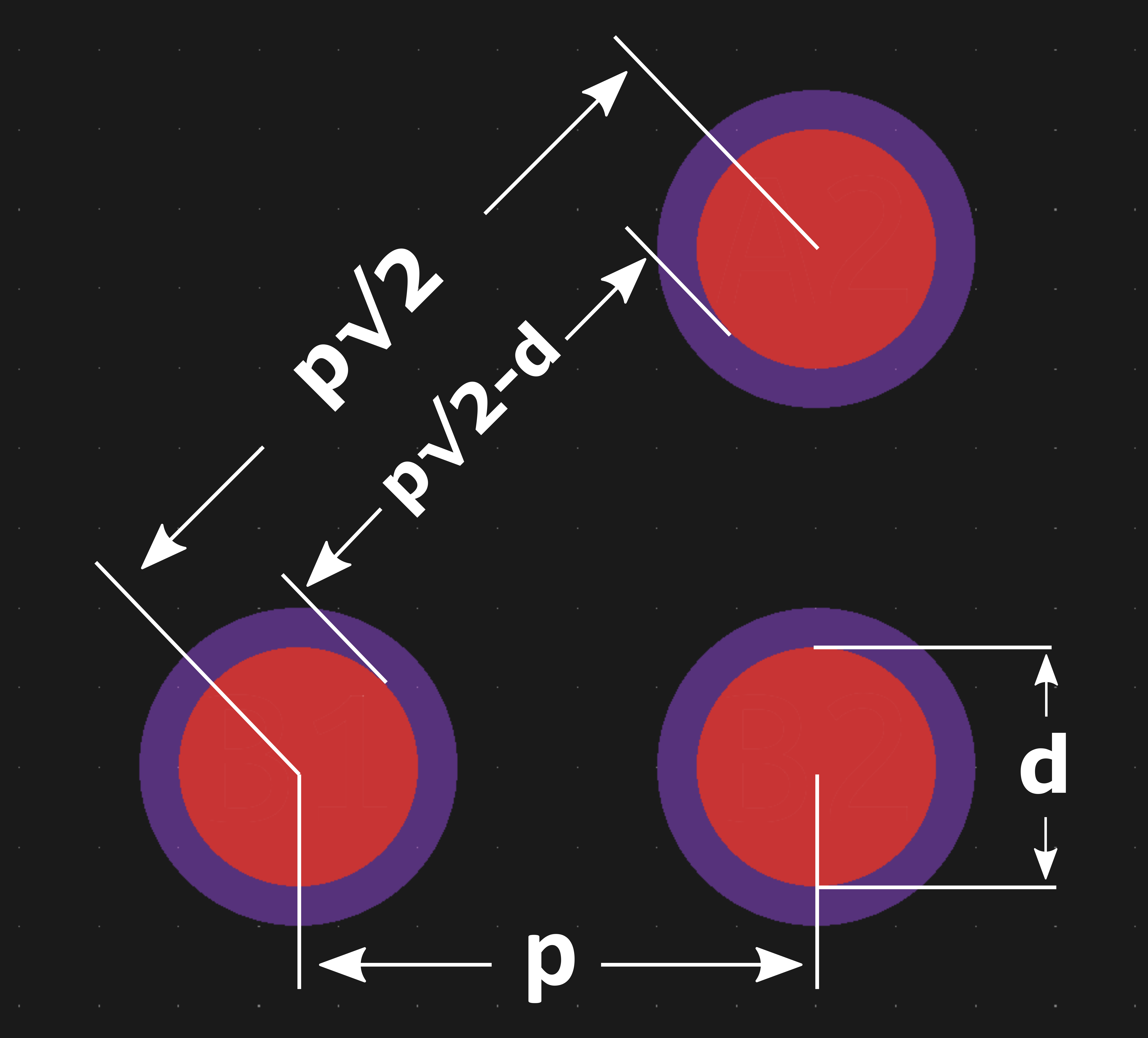
For the ATmega164, with p = 0.65 mm and d = 0.35 mm, this means we have 0.57 mm of space between the pads. We need to leave at least 0.1 mm of clearance between the pads and the via, so our maximum via size is 0.37 mm. This is pretty much on the limit of what most manufacturers can deliver; you can gain a little bit of room by moving the via slightly closer to the pad it’s connected to, but for smaller-pitch parts like this one you’ll have to go for the more expensive manufacturing options.
After placing the vias we end up with the layout shown below. This is the dog-bone layout style, named for the pad-trace-via combination that sort of looks like a cartoonish bone. In this simple case we only have nine dog-bones and plenty of space to route the signals on the bottom layer. If we had an 8×8 ball package instead, then we’d have sixteen dog-bones and the bottom layer would be just as crowded as the top layer.

The dog-bone layout style can be extended to any BGA size. But as the number of pads grows, the number of layers needed to route all the signals increases as well. A 7×7 or 8×8 BGA can be routed with just two signal layers, but a 9×9 or 10×10 chip needs at least three. In general, you need a new routing layer for every two additional rows of pads. In practice, many of the signals will be supply and ground pins that can directly connect to an internal power plane and don’t need further routing. There may also be unused pins, which again gives you a bit more routing space.
It’s important to ensure that all vias under your BGA chip are tented, or covered in solder mask. If they’re not, then the molten solder balls could flow onto the vias as well as the intended solder pads, causing misalignment and shorts. You’ll have to check with your PCB manufacturer if they support tented vias: this typically requires an additional processing step in which the via holes are filled with some material before the solder mask is applied.
BGA Routing: Via-in-Pad Layout
Another layout style for routing BGAs is via-in-pad. This is typically done for very fine pitch BGAs where you can’t fit a via between four pads. The basic idea is simple: you place one via inside each of the inner pads and route the signals outward from a lower layer. The problem is that you can’t simply place normal vias in your BGA pads, because the molten solder will be sucked inside the via hole through capillary action and cause unreliable joints. Your manufacturer will therefore need to fill the vias and apply a metal covering on top to ensure a flat, solderable surface. The official term for this is an IPC-4761 Type VII, Filled and Capped via.
The via holes need to be small enough to fit inside the BGA pad, and will usually end up being microvias: drilled by a laser rather than a mechanical drill. You can also simplify your routing by using blind vias, which don’t go all the way through the board but stop where you want them to. This is typically a costly option, but if your design uses the smallest Type VII microvias and the tightest clearance, then you’re probably already using the most expensive plan that includes blind vias anyway. Below is an example layout showing the via-in-pad technique applied to the TDC7201, although we wouldn’t typically need this on such a simple 25-pin device.
Whether you used the dog-bone or via-in-pad layout styles, once you’ve managed to bring all signals to the edge of your BGA (a process called “escape routing”) the rest of your PCB design will be almost as if you’d used a QFP or QFN package. The final result might look similar to the image shown at the top of this article.
As you can see, designing PCBs for small-to-medium sized BGA packages doesn’t have to be complicated. As long as the minimum trace pitch, clearance and via size offered by your PCB manufacturer are a good match for the pad size and pitch of the chips you’re planning to use, you’re all set. Classic BGAs with a 1.27 mm pitch will be doable at almost any manufacturer, while smaller chip-size packages with a pitch down to 0.65 mm typically need one of the more advanced processing options with tighter design rules.
The smallest wafer-level packages, with a ball pitch of 0.5 mm or smaller, can only be processed on the most advanced production lines. If you find yourself trying to design a PCB for such a small chip, it might be worthwhile to continue looking for that QFN or QFP version, because there’s little point in replacing an unobtainium chip with an unmanufacturable PCB.


Good article! Thank you!
+1 Community-Point for making it Kicad-aware.
There’s lots of info. More information than one pass, for me. I am bookmarking this to reread it for the next days.
Just remember the original BGA specification stated they were never intended to be larger than 1/2″ square. This was mostly due to the tremendous stress from a bimorph cantilever created with the underlying PCB. i.e. many modern production houses will limit the PCB thickness, and add under-chip adhesive to help mitigate solder ball failures.
There are only a few use-cases where BGA packages are necessitated, but with the nuisances they cause it is often the last option to choose. Personally, I prefer the exposed-pad QFN packages when possible. ;-)
It’s not really fair to call a device with this low a pitch (0.65 mm) a BGA. Traditional BGAs (0.8 mm+ pitch) are very reliable, even without underfill. Underfill helps lots of packages, not just BGAs – even TSOPs (0.5 mm pitch) aren’t terribly reliable under heavy stress.
CSPs definitely need underfill for reliability reasons but of course the size jump from a CSP to the typical QFN device is typically pretty huge, so it’s not really a fair comparison – tiny QFNs have their own issues too.
It’s more just “don’t use super-tiny devices unless you have to.”
Actually, I find the QFN have excellent production yields, and can mostly be visually inspected without xray equipment in many cases. And yes, fine pitch small things tend to move with surface tension unless glued down. However, the exposed pad QFN versions seem to self align in most cases.
Another issue I have with larger BGA, is they tend to cause intermittent temperature dependent physical failure modes. In a application where everything is shaking or temperature cycling, the localized PCB deformation can crack components or pull pads/balls under the BGA itself.
Sometimes one doesn’t get a choice with unicorn parts. And other times… if you can… sacrificing i/o pins for a more manageable IC is worth the compromise.
;-)
“Actually, I find the QFN have excellent production yields,”
Yes, because they’re larger. NASA has quite a bit of reliability data on QFN/BGA/CSP packages through NEPP. There’s an extremely strong die-to-package reliability relation – small package, worse reliability.
In fact on balance CSPs/BGAs can win out sometimes over QFNs because you can improve the strength of those packages via underfill. But in general it’s just a wash if you design it right.
“In a application where everything is shaking or temperature cycling,”
Everything fails in vibration/TSC tests, it’s just a question of when.
Last year when the shortages started I briefly toyed with the idea of messing around with an STM32G031 in CSP14. At .4mm pitch between the solder balls, as far as I can tell, common board fabs like OSHPark or JLCPCB simply can’t make something with such tight tolerances and advanced features like microvias or tented vias. Just for the heck of it I looked at pcbway just now. 5 20x20mm boards, 4 layers, .15mm minimum drill size, and via-in-pad costs over $300, versus the $5 or so a regular board costs. I’d be tempted to try it out at like $100, but at the estimated prices, yeesh.
The ball layout of the particular chip I was looking at was 4-3-4-3-4, and it meant if you could get away without using the inner 4 pins you could get away with much cheaper boards, you just need to be able to make small enough traces (and have sufficient accuracy with the soldermask, and so on. But larger stuff like 24-, 35- or larger pins? Effectively unobtanium, unless I missed something.
Good point Rick,
Most cheap board houses solder mask tolerances are far worse than the copper/drills DRC limits. We have seen many places simply knock out the finer pitch mask areas to get around the visibly sloppy alignment with the fiducial markers.
=)
Similar experience here – a lot of the micros & other chips that are left in stock are the ones that require an order of magnitude (or more) price increase in the PCB manufacturing.
Pitch goes the other way. When you have X somethings per Y units high pitch means bigger X.
I feel TSOP/TQFP packages would have a bit of an advantage in vibration and temperature-cycling environments, since the bend leads provide just a little bit of compliance. They can flex a few tens of microns, when non-compliant packages like BGAs and QFNs would develop cracks, especially with the brittle lead-free solder we have to use.
I don’t have any data to back this up, but this feels like an advantage for the leaded packages to me.
Mods please remove this bot, completely inappropriate and off topic
Two tricks I’ve found for working with BGAs by hand:
If possible, route minimum-width traces at 45 degrees off the corners of the package, and when placing the package, align to those. Silkscreen can suffer from layer registration issues, particularly at cheap board houses.
To inspect soldering, use something reflective at a 45 degree angle on the board surface so that the board can be kept flat on the bench for inspection. I used the chrome lid for my IPA dispenser, which has a nice natural curve on the edge, but there are other options, like a small piece of mylar. This will at least allow you to see if all the balls have compressed uniformly.
“One thing that will be of great help when assembling your PCB, especially if you’re doing it manually, is having the package outline indicated on your silkscreen layer.”
I prefer to put small square markers at the corners on the copper layer instead. In cheap PCB shops, the silkscreen location is often a bit inaccurate. With a 0.5 mm pitch BGA you can easily see the offset:
http://jpa.kapsi.fi/stuff/pix/jlcpcb_bga.jpg
I think most cheap PCB shops offer tented vias by default. The big issue for dogbone with many fabs will be the hole-to-hole and hole-to-trace specifications of the cheaper processes. For example, with JLCPCB, their “pad to track” (not exactly what we’re looking for, but the closest and most optimistic relevant spec from their sheet) tolerance is 0.2mm, which wouldn’t work with this dogbone configuration (2×0.2mm clearance + 0.2mm via + 2×0.13mm annular ring > 0.57mm). On the other hand, I’ve found that these fabs can, and usually will, do much more than their spec sheet advertises, but depending on how persnickety the person is that imports your gerbers, they may get rejected as out of spec.
One little trick that can be helpful if you are having issues with very tight BGA pitch and manufacturability is to use green solder mask when available. We have been told by board houses that the green solder mask is very heavily characterized and they can typically dial it in to much better tolerances than other colors of solder mask. Having looked at the apertures under a microscope, I can confirm that the green boards tend to look better. A prototype black solder mask board of the exact same design looked very sloppy in comparison.
Bad news for OSHPark?
If you need micro-BGA pitch it probably would get frustrating. Otherwise, probably not. YMMV
Not quite. I be able to get 0.4mm 6×6 BGA (ice40lp1k cm36) with ~32/36 (iirc) pads fanned out on 2 layers board. I don’t have a tool to physically measure the actual trace width. But in my design I used 3.5mil trace for fanning out. And the clearance of soldermask to pad is 0mil. I know it’s bad to violate multiple rules. But OSHpark, they are really capable. I believe that OSHpark 2 layers fab can goes down to sub 3mil trace. BtW, Here’s my project over OSHpark if you interested https://oshpark.com/shared_projects/ToirBVqj
https://oshpark.com/shared_projects/n9XXjf2W
One of the routines i used for large 1500 pin FPGA BGA’s went something like this. This technique was used on >12
layer boards with an autorouter. It went very briefly like this after component placement:
1. Fan out the whole FPGA BGA to a via-in-pad. Then run a secondary fan out on from the via-in-pad to a Core-Via ( a via which would span all inner layers and no outer layers) The core via is around 0.35mm. Now you effectively have turned and FPGA BGA package into a sort of hybrid through hole component package. Now Review (tidy up) and glue this fan out of PCB traces in place ( on mentor graphics it used to be called protect traces). This will stop the autorouter ripping them up and re-laying later.
2. You now then run another fan out on any SMD power smoothing caps and again review and then glue down. You now have a lot of you board components looking as thru hole parts. Now 50% of a large FPGA will be power rails and ground
return Rails. The other 50 % is all signal which is still left to route.
3. Now route in any critical analog AND/OR high speed sections to the FPGA;s . Something like high speed diff pairs and clocks distribution etc. Again glue and fix this down so no re-laying by the autorouter.
4. Now according to your timing parameters of your signals you can tell high end routers to keep within certain limits to route
the remaining interconnect.
This was used on large Network boxes and Telecoms boards around 1990’s to the 2010. All of the analog sections are usually hand routed and reviewed by analog engineers.
The FPGA BGA ‘s we were using were xilinx and they now have some good documentation on BGA fanout escapes from lower layer count to high layer count PCBs.
I think there are >2500 pin BGA’s but i have not worked on these.
Its not a golden bullet routine but it gives you and idea of some the processes used. If PCB layer count has to be low then
you have to get smarter and more interactive with the routing. If layer count is high then this can ease some of the pressure.
By the way you don’t have to have an autorouter but they are very good when tamed properly. We used to have standard scripts which ran different fan out sequences. It helped a lot with mundane tasks when used interactively.
Yep, thank you for the bunch of info. Not my day to day but definitely an article to keep in mind for reading when needed be.
I was always taught to not route signal layers on top of each other. But by taught I mean the internet, so is this wrong? Or is it 1 that this is just illustrative and the fan out pattern shows this for ease of visualization or 2 that most slow signals won’t be affected by this so it can safely be ignored most of the time, but it is good practice so it doesn’t bite you when you aren’t looking?
They’ve probably hidden the ground planes for the purposes of these screenshots. If you’re using BGA parts, you’re probably using at least a 4-layer board with at least one of the inner layers being a ground plane (the other is often a power plane) so the top (red) and bottom (blue) layers are quite well isolated from each other.
If you’re trying to squeeze 3 signal layers into a 4-layer board, those two adjacent layers are likely to have signal integrity problems.
These two Rick Hartley videos are great: https://www.youtube.com/watch?v=ySuUZEjARPY and https://www.youtube.com/watch?v=QG0Apol-oj0 — the tl;dw is that the energy of a trace is carried by the electric and magnetic fields between that trace and its return-current path (typically the ground path nearest the trace). The more you overlap the fields of two traces, the more cross-talk. E.g. if you have a signal trace on layer 1, a signal trace on layer 2, and a ground plane on layer 3, the fields associated with the trace on 1 will overlap with the fields associated with the trace on 2, so you’ll get cross-talk.
On that ATmega164, I’d “part” the tracks from the second layer of pins. B3 and B4 go LEFT and up, whiule B5 and B6 go RIGHT and up. This allows you to get one more track in per side (eg. between A4 and A5)
Now your 9 vias are down to 5.
You also want to connect GND pin D4 to one of the other GND pins, like A4 and / or G4.
very good, thank you !
You can add teardrops on the “dog bones” to improve PCB production yield. If the via hole is drilled too much off-center then it may cut the connecting track. Exaggerated pic:
https://piconomix.com/download/bga_dogbone_teardrop.png
You can also selectively remove via pads in the inner layers where it is not needed. This will allow for a more solid GND / PWR plane fill which is crucial!
https://piconomix.com/download/bga_pwr_plane_via_pads_removed.png
Finally, another an article worthy of HaD.
cool info, thanks; I plan to use some older BGAs, but for testing them, I got idea for deadly cheap burn ZIF using flexpcb on top of some flexible silicon/something layer … I modified KiCad BGA footprint generator to produce parametrized THT pads for balls, not for soldering them but only to align BGA there and push-it down against the silicon layer, hoping in ball connections in the micro-THT pads … not tested yet, but will try …