The news here isn’t so much that [Guarav Singh] built this high-quality industrial digital camera from scratch, but it’s in the way it was accomplished. That plus the amount of information that’s packed into the write-up, of course. And the excellent photography.
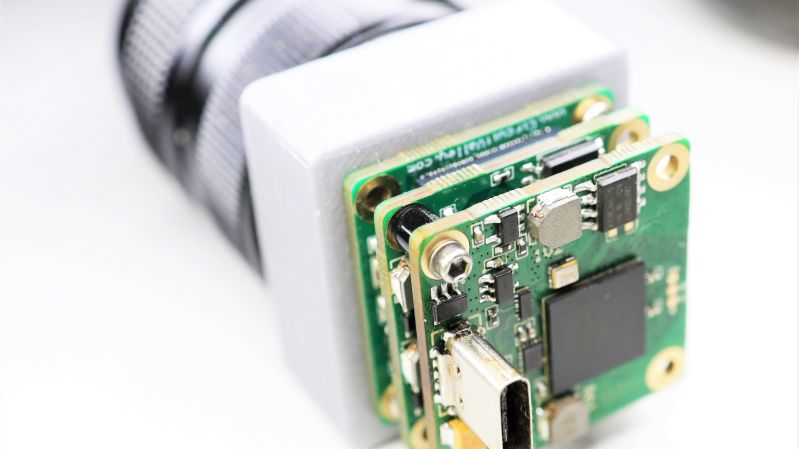
Modularity was one of [Guarav]’s design goals, with the intention of being able to swap out the sensor as the technology changes. To that end, [Guarav] came up with a stack of three PCBs. The middle board of the stack contains a Lattice FPGA chip along with two 16-MB RAMs and the FPGA config flash. The sensor board lies on one side of the FBGA board, while the USB 3.0 board is on the other. Each six-layer board is a masterpiece of high-density design, and the engineering that went into interfacing them and getting everything squeezed into a 3D-printed case with an integrated aluminum C-mount ring is pretty impressive.
[Guarav]’s write-up goes into a great deal of detail on processing the sensor data on the FPGA. Also, there’s quite a bit of practical information on implementing MIPI (Mobile Industry Processor Interface) and the CSI (Camera Serial Interface) specification. We’ve delved into this world before, but this project is a great hands-on explanation that might really help move your MIPI project along.
Thanks for the tip, [STR-alorman].


An impressive set of skills, and very nice execution and documentation!
+1 to that. really impressive project.
I wonder what the full build cost is?
That’s very well done and easy to follow. I recently took apart a Unifi Video Doorbell and it used a similar concept of stacked PCBs though on a smaller scale.
Looking at the 3D printed lens mount, I’d have some concerns about that CS mounting ring popping out since it appears to be press fit. I would either make it captive or make the mount 2 part and sandwich it in the middle. That’s just my armchair analysis though.
Ok. Now that we know how to make it, how about how to buy it?
i applaud the effort but come on man max 2.13mpix CMOS sensor with C-mount???? that’s like early 1990 tech…..
rolling shutter is nice and all but CCD sensors are so much better overall nowaday. you can find arduino/rpi 12-20mpix modules for about 50-60$ as well as industrial c-mount modules starting at 20$ so yeah nice experiment but i don’t really see the practical use.
The whole point of this is modularity. There are lots of csi sensors out there. For my use case (super low latency imaging) this would be huge. I’ve been waiting for something like this I can tinker with without making my own hardware for years. Even with 2Mpix camera. All Sbcs have essentially a black box camera processing pipeline that adds 40~100ms of latency which makes them essentially unusable for projects that interest me, where I need a maximum of 10ms latency(ideally less).
In case you’re still reading this: I used to work with so called event cameras like the IMX636 which provide very low latencies (easily <1ms, at least in theory). The downside is that you don't get full frames, but partial, differential updates. Maybe that's an option for your project? Feel free to contact me or reply here if so.
I’d love to buy it if it was up to $250.