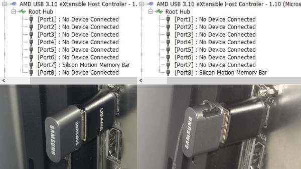
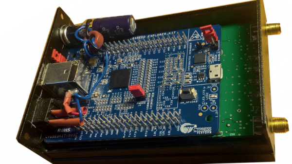
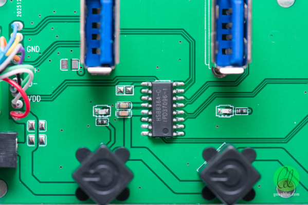
All About USB-C: High-Speed Interfaces

One amazing thing about USB-C is its high-speed capabilities. The pinout gives you four high-speed differential pairs and a few more lower-speed pairs, which let you pump giant amounts of data through a connector smaller than a cent coin. Not all devices take advantage of this capability, and they’re not required to – USB-C is designed to be accessible for every portable device under the sun. When you have a device with high-speed needs exposed through USB-C, however, it’s glorious just how much USB-C can give you, and how well it can work.

The ability to get a high-speed interface out of USB-C is called an Alternate Mode, “altmode” for short. The three altmodes you can encounter nowadays are USB3, DisplayPort and Thunderbolt, there’s a few that have faded into obscurity like HDMI and VirtualLink, and some are up and coming like USB4. Most altmodes require digital USB-C communication, using a certain kind of messages over the PD channel. That said, not all of them do – the USB3 is the simplest one. Let’s go through what makes an altmode tick. Continue reading “All About USB-C: High-Speed Interfaces”

Showing the same thumbdrive plugged into the same USB-C port in two different orientations, enumerating as two different USB ports

Dirty USB-C Tricks: One Port For The Price Of Two

[RichardG] has noticed a weird discrepancy – his Ryzen mainboard ought to have had fourteen USB3 ports, but somehow, only exposed thirteen of them. Unlike other mainboards in this lineup, it also happens to have a USB-C port among these thirteen ports. These two things wouldn’t be related in any way, would they? Turns out, they are, and [RichardG] shows us a dirty USB-C trick that manufacturers pull on us for an unknown reason.

On a USB-C port using USB3, the USB3 TX and RX signals have to be routed to two different pin groups, depending on the plugged-in cable orientation. In a proper design, you would have a multiplexer chip detecting cable orientation, and routing the pins to one or the other. Turns out, quite a few manufacturers are choosing to wire up two separate ports to the USB-C connector instead.

In the extensive writeup on this problem, [Richard] explains how the USB-C port ought to be wired, how it’s wired instead, shows telltale signs of such a trick, and how to check if a USB-C port on your PC is miswired in the same way. He also ponders on whether this is compliant with the USB-C specification, but can’t quite find an answer. There’s a surprising amount of products and adapters doing this exact thing, too, all of them desktop PC accessories – perhaps, you bought a device with such a USB-C port and don’t know it.

As a conclusion, he debates making an adapter to break the stolen USB3 port out. This wouldn’t be the first time we’re cheated when it comes to USB ports – the USB2 devices with blue connectors come to mind.

Scratch-Built Industrial Camera’s Modular Design Really Stacks Up

The news here isn’t so much that [Guarav Singh] built this high-quality industrial digital camera from scratch, but it’s in the way it was accomplished. That plus the amount of information that’s packed into the write-up, of course. And the excellent photography.

Modularity was one of [Guarav]’s design goals, with the intention of being able to swap out the sensor as the technology changes. To that end, [Guarav] came up with a stack of three PCBs. The middle board of the stack contains a Lattice FPGA chip along with two 16-MB RAMs and the FPGA config flash. The sensor board lies on one side of the FBGA board, while the USB 3.0 board is on the other. Each six-layer board is a masterpiece of high-density design, and the engineering that went into interfacing them and getting everything squeezed into a 3D-printed case with an integrated aluminum C-mount ring is pretty impressive.

[Guarav]’s write-up goes into a great deal of detail on processing the sensor data on the FPGA. Also, there’s quite a bit of practical information on implementing MIPI (Mobile Industry Processor Interface) and the CSI (Camera Serial Interface) specification. We’ve delved into this world before, but this project is a great hands-on explanation that might really help move your MIPI project along.

Thanks for the tip, [STR-alorman].

Top side of the VL670 breakout board, with two USB connectors and the VL670 chip in the center.

A Chip To Bridge The USB 2 – USB 3 Divide

On Twitter, [whitequark] hasĀ  found and highlighted an intriguing design – a breakout board for the VL670, accompanied by an extensive yet very easy to digest write-up about its usefulness and inner workings. The VL670 is a chip that addresses a surprising problem – converting USB 2.0 signals into USB 3.0.

If you have a USB 2.0 device and a host with only USB 3.0 signals available, this chip is for you. It might be puzzling – why is this even needed? It’s about the little-known dark secret of USB3, that anyone can deduce if they ever have to deal with a 9-pin USB 3.0 connector where one of the three differential pairs doesn’t quite make contact.

When you see a blue “3.0” port, it’s actually USB 2 and USB 3 — two separate interfaces joined into a single connector. USB 3 uses two single-directional differential pairs, akin to PCI-E, whereas USB 2 uses a single bidirectional one, and the two interfaces on a blue connector operate basically independently of each other. There’s many implications to this that are counterintuitive if you simply take “USB 3.0” for “faster backwards-compatible USB”, and they have painful consequences.

For instance, USB 3 hub ICs have two separate hub entities inside – one for USB 3 and one for USB 2. Even if you have a USB 3 hub plugged into a USB 3 port, multiple USB 2 devices plugged into it still cannot break through the USB 2 uplink limit of 480 MBps. If you ever thought that a faster hub with a faster uplink would fix your USB 2 device speed problems – USB-IF engineers, apparently, thought differently; and you might have to find a workaround for your “many cheap SDRs and Pi 4 in a box” setup. Continue reading “A Chip To Bridge The USB 2 – USB 3 Divide”

Spite, Thrift, And The Virtues Of An Affordable Logic Analyzer

[Larry Wall], the father of Perl, lists the three great virtues of all programmers: Laziness, Impatience, and Hubris. After seeing that Saleae jacked up the prices on their popular logic analyzers to ludicrous levels, [CNLohr] added a fourth virtue: Spite. And since his tests with a Cypress FX3 over the last few days may lead to a dirt-cheap DIY logic analyzer, we may soon be able to add another virtue: Thrift.

The story begins a year or two ago when [CNLohr] got a Cypress FX3 development board for $45. The board sat unused for want of a Windows machine, but after seeing our recent article on a minimalist logic analyzer based on an FX2, he started playing with the board to see if it could fan the flames of his SaleaeĀ hatred. The FX3 is a neat little chip that has a 100-MHz General Programmable Interface (GPIF) bus that basically lets it act like an easy to use FPGA.

Prepared to spend months on the project, he was surprised to make significant progress on his mission of spiteful thrift within a few days, reading 16 bits off the GPIF at over 200 megabytes per second and dumping it over the USB 3.0 port. [Charles]’ libraries for the FX3 lay the foundation for a lot of cool stuff, from logic analyzers to SDRs and beyond — now someone just has to build them.

The search for a cheap but capable logic analyzer is nothing new, of course. Last year, both [Jenny List] and [Bil Herd] looked at the $22 iCEstick as a potential Saleae beater.

Continue reading “Spite, Thrift, And The Virtues Of An Affordable Logic Analyzer”

The Breadboard RF103

When [ik1xpv] sets out to build a software-defined radio (SDR), he doesn’t fool around. His Breadboard RF103 sports USB 3.0, and 16-bit A/D converter that can sample up to 105 Msps, and can receive from 0 to 1800 MHz. Not bad. Thanks to the USB 3.0 port, all the signal processing occurs in the PC without the limitations of feeding data through a common sound port. You can see the device in action in the video below.

The Cypress FX3 USB device is an ARM processor, but it is only streaming data, not processing it. You can find the slightly modified firmware, a driver for using PC software, and schematics and board layouts on GitHub.

Continue reading “The Breadboard RF103”