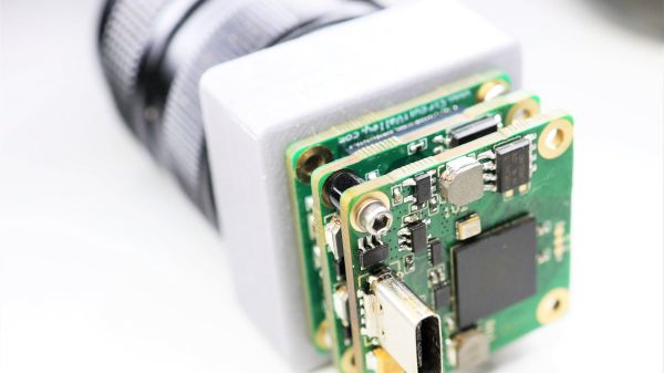
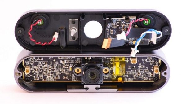
The Kodak Charmera is a tiny keychain camera produced by licencing out the name of the famous film manufacturer, and it’s the current must-have cool trinket among photo nerds. Inside is a tiny sensor and a fixed-focus M7 lens, and unlike many toy cameras it has better quality than its tiny package might lead you to expect. There will always be those who wish to push the envelope though, and [微攝 Macrodeon] is here to fit a lens mount for full-size lenses (Chinese language, subtitle translation available).
The hack involves cracking the camera open and separating the lens mount from the sensor. This is something we’re familiar with from other cameras, and it’s a fiddly process which requires a lot of care. A C-mount is then glued to the front, from which all manner of other lenses can be attached using a range of adapters. The focus requires a bit of effort to set up and we’re guessing that every lens becomes extreme telephoto due to the tiny sensor, but we’re sure hours of fun could be had.
The Charmera is almost constantly sold out, but you should be able to place a preorder for about $30 USD if you want one. If waiting months for delivery isn’t your bag, there are other cameras you can upgrade to C-mount.


