37C3: When Apple Ditches Lightning, Hack USB-C

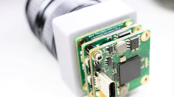
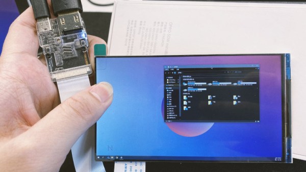
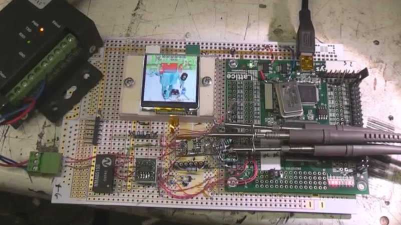
[Thomas Roth], aka [Ghidraninja], and author of the [Stacksmashing] YouTube channel, investigated Apple’s Lightning port and created a cool debugging tool that allowed one to get JTAG on the device. Then, Apple went to USB-C for their new phones, and all his work went to waste. Oh well, start again — and take a look at USB-C.

Turns out, though, that the iPhone 15 uses the vendor-defined messages (VDM) capability of USB-PD to get all sorts of fun features out. Others had explored the VDM capabilities on Mac notebooks, and it turns out that the VDM messages on the phone are the same. Some more fiddling, and he got a serial port and JTAG up and running. But JTAG is locked down in the production devices, so that will have to wait for an iPhone 15 jailbreak. So he went poking around elsewhere.

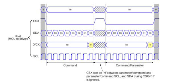
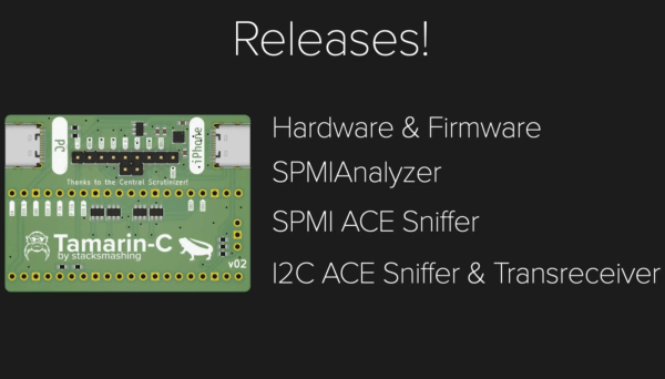
He found some other funny signals that turned out to be System Power Management Interface (SPMI), one of the horribly closed and NDA-documented dialects owned by the MIPI Alliance. Digging around on the Interwebs, he found enough documentation to build an open-source SPMI plugin that he said should be out on his GitHub soon.

The end result? He reworked his old Lightning hardware tool for USB-C and poked around enough in the various available protocols to get a foothold on serial, JTAG, and SPMI. This is just the beginning, but if you’re interested in playing with the new iPhone, this talk is a great place to start. Want to know all about USB-C? We’ve got plenty of reading for you.

Scratch-Built Industrial Camera’s Modular Design Really Stacks Up

The news here isn’t so much that [Guarav Singh] built this high-quality industrial digital camera from scratch, but it’s in the way it was accomplished. That plus the amount of information that’s packed into the write-up, of course. And the excellent photography.

Modularity was one of [Guarav]’s design goals, with the intention of being able to swap out the sensor as the technology changes. To that end, [Guarav] came up with a stack of three PCBs. The middle board of the stack contains a Lattice FPGA chip along with two 16-MB RAMs and the FPGA config flash. The sensor board lies on one side of the FBGA board, while the USB 3.0 board is on the other. Each six-layer board is a masterpiece of high-density design, and the engineering that went into interfacing them and getting everything squeezed into a 3D-printed case with an integrated aluminum C-mount ring is pretty impressive.

[Guarav]’s write-up goes into a great deal of detail on processing the sensor data on the FPGA. Also, there’s quite a bit of practical information on implementing MIPI (Mobile Industry Processor Interface) and the CSI (Camera Serial Interface) specification. We’ve delved into this world before, but this project is a great hands-on explanation that might really help move your MIPI project along.

Thanks for the tip, [STR-alorman].

How To Drive Smartphone Screens Over HDMI

Compared to most small LCDs sold to makers, smartphone screens boast excellent color, brightness, and insanely high resolution. Unfortunately, driving them is rarely straightforward. In an attempt to make it easier, [peng-zhihui] set about developing tools to allow such screens to be driven from a simple HDMI feed. For those whose Chinese is a little rusty, the Google Translate link might prove useful.

The first attempt was using Toshiba’s TC358870XBG ASIC, capable of driving screens over MIPI DSI 1.1 from an HDMI input. [peng-zhihui] designed a simple test module for the chip based on the company’s evaluation board design, with [ylj2000] providing software to help get that solution off the ground.

However, for now that solution is imperfect, so [peng-zhihui] also experimented with the Longxun LT6911 HDMI to MIPI driver. While cheap, information on the part is scarce, and the company’s own source code for using the hardware is only accessible by signing an NDA. However, [peng-zhihui] made pre-compiled firmware available for those that wish to work with the hardware.

[peng-zhihui] has put these learnings to good use, building a power bank with a MIPI screen using what appears to be the Longxun chip. The device can supply power over USB and also act as an HDMI display.

While it’s early days yet, and driving these screens remain difficult, it’s great to see hackers getting out there and finding a way to make new parts work for them. We’ve seen similar work before, using an FPGA rather than an off-the-shelf ASIC. If you’ve found your own way to get these high-end displays working, be sure to drop us a line!

[Thanks to peterburk for the tip!]

Xilinx Makes MIPI CSI And DSI Controller IP Blocks Free To Use With Vivado

If you want to use a display or camera with an FPGA, you will often end up with a MIPI-based solution. As of the Xilinx Vivado 2020.1 release, the MIPI DSI (display serial interface) and CSI (camera serial interface) IP blocks are now bundled with the IDE to be used freely with Xilinx FPGAs.

The Xilinx MIPI CSI2 receiver block implements the CSI-2 v1.1 specification, which although a bit older is essentially the same CSI implementation as on the Raspberry Pi boards. This means that it would allow one to use this IP block on an FPGA with many common CSI camera modules out there. The IP block offers a standard AXI4 interface for connecting up to the rest of a design.

Similarly, the Xilinx MIPI DSI transmitter block implements DSI v1.3 specification. This offers a maximum data rate of 1.5 Gbps, with an AXI4-lite interface to communicate with the rest of the design. Both IP blocks are subject to the Core license agreement, which doesn’t appear to preclude it from being used in a specific fashion, whether commercial or personal.

This is not the only way to use MIPI devices with an FPGA, of course. Take for example [Daveshah]’s CSRIx project on Github.

Header image: Kwapix / CC BY-SA 4.0

Speeding Up Drawing To MCU-Connected Serial Displays

Writing image data to serially connected (SPI/I2C) displays from a microcontroller is easy enough these days, courtesy of standards defined by the MIPI Alliance, yet there are some gotchas in it which may catch someone using it unaware. [Larry Bank] wrote up a good summary of how one can get maximum performance out of such a display link.

At the core is the distinction between pixel data and command transmissions. The change from command to pixel data mode requires signaling, which takes precious clock cycles away from transferring pixel data between the MCU and display. The common MIPI DCS instruction set allows for a big reduction in needed data transfers by allowing parts of the display to be addressed instead of requiring a full refresh. Yet by not properly segmenting command and data transfers, one ends up unnecessarily slowing down the process.

The result is that one can run something like a Pac-Man emulator on an AVR MCU with a sluggish 320×480 SPI LCD at 60 FPS, as one can see in the video that is embedded after the break. Check the article for another demo video as well.

Continue reading “Speeding Up Drawing To MCU-Connected Serial Displays”

Putting An Out Of Work IPod Display To Good Use

[Mike Harrison] produces so much quality content that sometimes excellent material slips through the editorial cracks. This time we noticed that one such lost gem was [Mike]’s reverse engineering of the 6th generation iPod Nano display from 2013, as caught when the also prolific [Greg Davill] used one on a recent board. Despite the march of progress in mobile device displays, small screens which are easy to connect to hobbyist style devices are still typically fairly low quality. It’s easy to find fancier displays as salvage but interfacing with them electrically can be brutal, never mind the reverse engineering required to figure out what signal goes where. Suffice to say you probably won’t find a manufacturer data sheet, and it won’t conveniently speak SPI or I2C.

After a few generations of strange form factor exploration Apple has all but abandoned the stand-alone portable media player market; witness the sole surviving member of that once mighty species, the woefully outdated iPod Touch. Luckily thanks to vibrant sales, replacement parts for the little square sixth generation Nano are still inexpensive and easily available. If only there was a convenient interface this would be a great source of comparatively very high quality displays. Enter [Mike].

Outer edge of FPGA and circuit

This particular display speaks a protocol called DSI over a low voltage differential MIPI interface, which is a common combination which is still used to drive big, rich, modern displays. The specifications are somewhat available…if you’re an employee of a company who is a member of the working group that standardizes them — there are membership discounts for companies with yearly revenue below $250 million, and dues are thousands of dollars a quarter.

Fortunately for us, after some experiments [Mike] figured out enough of the command set and signaling to generate easily reproduced schematics and references for the data packets, checksums, etc. The project page has a smattering of information, but the circuit includes some unusual provisions to adjust signal levels and other goodies so try watching the videos for a great explanation of what’s going on and why. At the time [Mike] was using an FPGA to drive the display and that’s certainly only gotten cheaper and easier, but we suspect that his suggestion about using a fast micro and clever tricks would work well too.

It turns out we made incidental mention of this display when covering [Mike]’s tiny thermal imager but it hasn’t turned up much since them. As always, thanks for the accidental tip [Greg]! We’re waiting to see the final result of your experiments with this.

MIPI CSI-2 Implementation In FPGAs

[Adam Taylor] always has interesting FPGA posts and his latest is no exception. He wanted to use a Zynq for image processing. Makes sense. You can do the high-speed parallel parts in the FPGA fabric and do higher-level processing on the built-in CPU. The problem is, of course, you need to get the video data into the system. [Adam] elected to use the Mobile Industry Processor Interface (MIPI) Camera Serial Interface Issue 2 (CSI-2).

This high-speed serial interface is optimized for data flowing in one direction. The camera, or the master, sends a number of bits (at least one) serially with one clock. To increase speed, data transfers on both rising and falling clock edges. The slave also has a pretty standard I2C master to send commands to the camera which, for the purposes of I2C, is the slave.

Continue reading “MIPI CSI-2 Implementation In FPGAs”