[James Sharman] has been working away on a 8-bit CPU of his own design. Naturally, with his computing device largely functional, the obvious question was asked: can it run DOOM? [James’] latest video explores this question, showing just how close he was able to get.
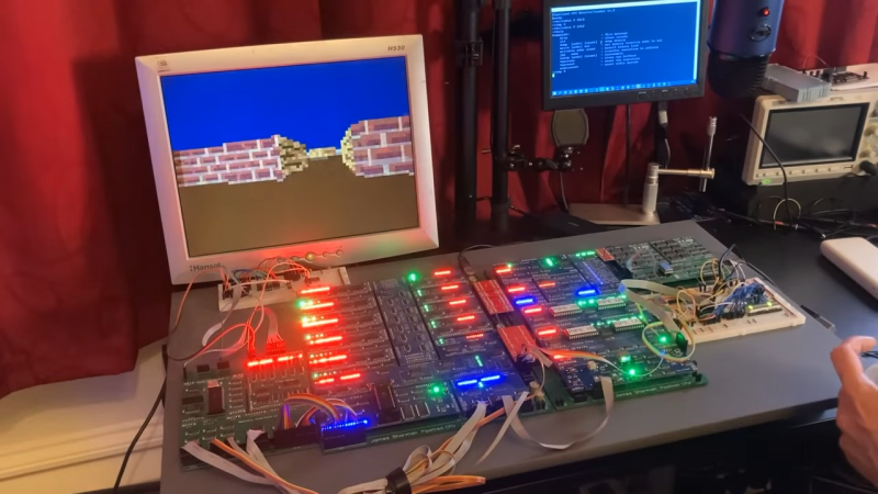
[James’] 8-bit pipelined CPU also has its own UART, VGA adapter, and sound adapter all built up on discrete components on various PCBs. There’s also a custom interface for a SNES controller as an input device. However, it’s fundamentally well below the specs that DOOM originally required at launch. His 8-bit CPU runs at just 4 MHz, with 64 KB of RAM. This compares poorly to the 32-bit, 33 MHz Intel 386 chips and 4 MB of RAM originally recommended to run the game.
In lieu of running the real thing, [James] demonstrated the limitations of his machine by coding his own demo, nicknamed Doomed. It’s able to average 19 fps video output at a resolution of 80×60, and consists of over 5,000 lines of hand-written assembly code. Fundamentally, it’s a basic 3D engine not dissimilar to Wolfenstein 3D, though without any actual gaming interactions involved.
[James] could have simply stated the machine won’t run DOOM. However, trying to get something similar up and running was a useful learning experience, and in his own words, highly satisfying. This attitude of pushing on in the face of adversity is what propels many other DOOM porting efforts.
[Thanks to Keith Olson for the tip!]


Homebrew CPUs are something special
This is excellent! I wonder if James has looked at putting it in as a demoscene entry ? 😊
Yeah he should enter the wild competition @Revision 2023!
I was going to suggest porting the SNES code but then I realized it uses a SuperFX chip. However, they could take a page from the TI-83 recreation of DOOM. To be honest, adding a rudimentary GPU (only accelerate one or two things) seems like the most viable path.
This is a real Hack, worthy of being on Hack-A-Day!
” it’s a basic 3D engine not dissimilar to Wolfenstein 3D, though without any actual gaming interactions involved ”
Then is it Doom or is it ? …
https://www.youtube.com/watch?v=oRL5durPleI
I’d be interested in knowing more about the hardware. How many cycles does a typical instruction require? What’s the instruction set? What’s limiting the speed to 4 MHz?
Ditto
I found this. Not sure if it’s from the author.
https://github.com/jamon/jamessharman-8bit-cpu-sim
Jamon is in James’ Discord server and is one of several members working on a simulator. Another one is https://github.com/Artentus/Pipelined-CPU-Emu
The instruction set is a completely custom one. There are 256 opcodes. Instructions generally take 1 cycle, as this is a 2 stage (+ fetch) pipelined design. Jumps and memory ops take 2 cycles. So he runs just under 4 MIPS at 4 MHz. He has plans to do some analysis to determine what exactly is the limiting factor on the clock speed. Essentially, the clock rate is limited by the critical path, which is the longest propagation chain through the TTL chips. Based on my own homebrew design, and being familiar with his, I’d hazard a guess that his critical path is reading or writing the Memory Bridge, which is the transceiver that connects the internal Main Bus to the external Memory Data bus. So essentially he is likely limited by how long his RAM needs to read or write, combined with how far into the cycle it has to wait until data is stable on the mem data / main buses.
Thanks. From your explanation and the github links above, leading to his youtube videos, I learned that he gets roughly 0.75 instructions per clock. The design is mostly standard 74 series TTL, which puts severe limits on how much speed is possible even if RAM is very fast.
This is really impressive work.
Awesome Build!