Not that long ago, rolling your own printed circuit boards was difficult, time-consuming and expensive. But thanks to an army of cheap, online manufacturing services as well as high-quality free design software, any hobbyist can now make boards to rival those made by pros. A similar shift might be underway when it comes to chip design: affordable manufacturing options and a set of free software tools are slowly bringing custom chips into the realm of hackers and hobbyists. One of those working hard to democratize chip design is Matt Venn, who’s been telling us all about his current big project, called Tiny Tapeout, in his talk at Remoticon 2022.
Matt’s quest to bring IC design to the masses started in 2020, when the first open-source compatible Process Design Kit (PDK) was released to the public. A PDK is a collection of files, normally only available under strict non-disclosure agreements, that describe all the features of a specific chip manufacturing process and enable you to make a design. With this free PDK in hand and a rag-tag collection of free software tools, Matt set out to design his first chip, a VGA clock, which he taped out (released to manufacturing) in July 2020.
Building on this experience, Matt wrote a complete beginner’s guide to chip design, called the Zero to ASIC course. To give students the opportunity to put this theory into practice, he also organized a multi-project wafer: a single manufacturing run that pools multiple designs in order to split the cost. This turned out to be hugely popular, and Matt has so far coordinated seven of these MPWs, each with loads of interesting designs.
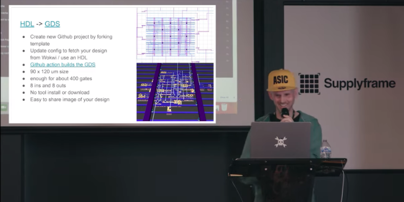
However, even with a free PDK, open-source tools and a detailed course explaining the way, designing properly functioning chips is still very difficult. Matt’s next big project, called Tiny Tapeout, therefore aims to make chip design so easy that even a child can do it. It does this by integrating all the required tools into a single web-based application and offering a cheap manufacturing option to go with it.
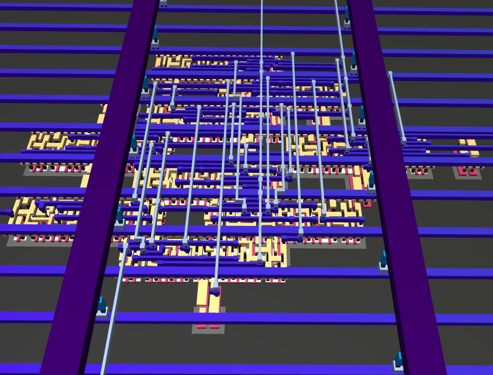
The web tool is based on WokWi by Uri Shaked. WokWi is a browser-based circuit simulation tool, originally developed for Arduino programming, which Matt and Uri turned into a logic design and simulation tool for chip design. Once you’ve designed your chip’s logic behavior, you can link the design into a GitHub repository where a script will then turn it into a complete chip layout. You can view the layout and even zoom around the transistors in a full 3D view, seeing exactly what the final result would look like under a microscope.
On the manufacturing side, Matt provides each project with a chip area of 90 by 120 microns, enough for around 400 logic gates. Each chip gets eight inputs and eight outputs, which can operate at clock frequencies of up to 15 kHz. This might not seem like much, but the project’s trial run yielded several impressive projects, including simple counters and adders but also a 4-bit CPU and even a 9-LUT FPGA.
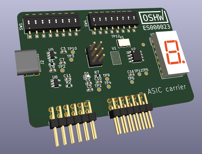
There’s space on the chip for about 500 different designs, all of which will be present in all manufactured chips – you can choose which design is active by selecting the ID of that design using DIP switches on the PCB. A comprehensive datasheet will list the contents of each single design, so there’s plenty left to play with even after you’ve checked out your own work.
Matt also has lots of things left to do: he’s aiming to add analog and RF functionality to the current design flow, which would enable far more versatile designs that can connect to sensors and drive high-speed data buses. One tool that will help in teaching analog design is SiliWiz, another web-based simulation tool he’s been working on that lets you play with on-chip transistor layouts and see their electrical behavior in real time.
We can’t help but be impressed by Matt’s tireless work to make chip design available to anyone, and we’re looking forward to the next, even more powerful generation of Tiny Tapeout. Perhaps one day, submitting a GDS file to a fab will seem just as ordinary as sending Gerbers to a PCB shop is today.


The max clock is 25kHz
https://github.com/TinyTapeout/tinytapeout-02/raw/tt02/datasheet.pdf
I was wondering why so low and the reason is the whole chip is linked into a long scan chain that links all the 500 designs and so each individual one is updated when it’s turn comes.
That’s the 250 design version, hence the reason why the clock is 2x as fast. The assumption they’re using is that the scan chain will run at 100 MHz, 8 inputs, 2 clocks per input. So 250 designs gives you a 25 kHz update, 500 gives you 12.5 kHz update.
The clarification that’s sometimes missing is that this is a multi-project die that’s also built on a multi-project wafer. With a multi-project wafer, they combine a bunch of different dice on one wafer, and then cut up the wafer and you get your dice. With this, you get one chip (a packaged die) that contains all the projects, even those that aren’t yours.
I’m really curious about the idea for analog, I don’t know how you’d do that.
Seems it would increase mask complexity.
They talk about it here:
https://resourcecenter.sscs.ieee.org/education/webinars/SSCSWEB4065.html
IEEE SSCS is working on a new analog setup
Analog is harder as to make it safe we have to do power isolation, and to make it useful we need to keep noise low and provide separate power supplies. I’m working with a couple of very experienced analog designers to trial some ideas this year. It won’t be soon but it’s being worked on.
I knew I should’ve been clearer: I actually meant how do you plan on doing analog input/output? Obviously you can’t mux it like you’re doing for digital. Or is it just predefined blocks or something?
I’ve worked with colleagues who’ve done a similar multi-function die in an MPW years ago, but that was only like 7 different structures, not hundreds.
Although I guess a smart thing would be to have a smaller number of analog blocks which have the dedicated output, and keep the digital interface. Most of the analog ASICs we have we don’t really care if the digital configuration stuff is super-slow since it’s rare.
Why not mux after the conversion to digital? Alternatively, you could have dumb busses that drive or are driven by simple PWM or repeating serial with sync sequences. You’d need tri-state IO that goes high-impedance when a project isn’t active.
Any analog muxing will really limit performance. It won’t make it useless or anything, but not RF level stuff. Any internal bus spread to hundreds of blocks will have parasitics limiting you to MHz or worse.
It’s just lots of tradeoffs, and a question of what you’re trying to do.
A) Is this only for standard cell designs? B) are small RAM arrays part of the library? C) I’m sure everyone is thinking that a good clock distribution tree would be most welcome. Looking forward to hearing more about TTO3’s MUXed I/O approach too. Regardless of the early limitations, all steps in the right direction. Kudos!
Does he provide a diagram?
I’ll see myself out.
You beat me to it.
Hey, thanks for the writeup! Just a couple of clarifications – I don’t organise the MPWs, that’s Efabless & Google. I have just taken part in them. They are free to enter, and run as a lottery.
TinyTapeout guarantees silicon by buying a single slot on an MPW and then sharing that between a few hundred people.
TinyTapeout 1 & 2 both used a scan chain and hence the slow update frequency. Tiny Tapeout 3 (opening in a few weeks) has moved to a mux based design that should get us into a few MHz at least.
What makes this more economical than an FPGA implementation?
It’s all about volume. If you only need to make a small number then FPGAs are cheaper, if you are mass manufacturing then having chips manufactured will be cheaper. Additionally if you fab your own chip you can achieve higher clock rates than FPGAs can normally provide
I know the advantage of having your own chip I am just not sure this particular process is viable commercially since it can only do 15Khz. Educational yes it is good way to practice.
It’s just the interface that runs that slow. Internally the logic can be very fast, which means you can nominally use this to test designs cheaply.
If you look just above this comment you’ll see that Matt Venn stated that it was so slow due to an architectural decision to scan through each project. He says the next go-round should use mux’d selection of the project, which should bring operating frequency into the low-MHz range.
I don’t think economy is the point. There is plenty of web-based information on the crossover point between FPGAs and ASICs. This is an incredible effort to develop the specialized skills for ASIC design in an affordable way.
“More economical than an FPGA” isn’t the point, but this is a heck of a lot more economical than getting your own chunk-of-wafer, because the chunk is further subdivided.
I have a long history of circuit design background (ASIC, FPGA, etc.) and this TinyTapeout project is profoundly game changing. “Democratizing ASICs” says it all…
Ya coulda cut out the loud burst of static before uploading to YouTube, ya lazy sons of mothers! 😠
Holy smokes!
Icarus vlog sim useful