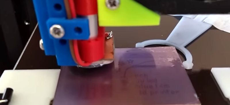
Do you ever wonder why your PCB maker uses Gerber files? It doesn’t have to do with baby food. Gerber was the company that introduced photoplotting. Early machines used a xenon bulb to project shapes from an aperture to plot on a piece of film. You can then use that film for photolithography which has a lot of uses, including making printed circuit boards. [Wil Straver] decided to make his own photoplotter using a 3D printer in two dimensions and a UV LED. You can see the results in the video below.
A small 3D printed assembly holds a circuit board, the LED, and a magnet to hold it all to the 3D printer. Of course, an LED is a big large for a PCB trace, so he creates a 0.3 mm aperture by printing a mold and using it to cast epoxy to make the part that contacts the PCB film.
The fan control turns the LED on and off, much as laser cutter mods for 3D printers often do. We noticed he uses standard nuts as heat set inserts, and that seems to work well enough, especially since there isn’t much load on them in this application. There were a few iterations of pinholes and mounts, but the final iteration seems to work well. There is even a method to do double-sided boards.
Of course, with a laser cutter and good focusing, you could pull the same trick. Just be aware that some of the “high power” laser modules don’t focus to a dot because of their internal construction. Turns out, there’s more than one way to have a printer help you with PCB production.


This is such beautiful Art!
I can’t recall if I have seen this done, or just invented it :-)
But it seems that you should be able to lay down a single layer of conventional filament as a resist and then etch normally?
But then you need to expend filament and do extra steps
These were around very early in PCB technology.
https://en.wikipedia.org/wiki/Photoplotter
The RS-274X standard starts to make sense when you understand what Gerber did in these plotters.
Probably before your time, and was replaced with faster processes decades ago =)
Sorry, I went off on a bit of a tangent, I wasn’t really talking about the main thrust of the article just speculating on other ways to use a 3D printer.
I haven’t used a photoplotter, but I did use a phototypwsetter extensively when I was a student.
This would produce long strips of text (All the same font and size, as far as I rememeber) that we then pasted down to make the lithography masters.
It was, in some ways, better than what we have now. You could put the text anywhere you wanted, at any angle.
I don’t see why not – your track width would be the nozzle aperture or a bit wider (typ 0.4 mm).
The filament would have to adhere well and resist the etchant so that it doesn’t come off when processing. And You’d have to have some way to remove the filament afterwards that wouldn’t damage the PCB. If there is a filament that meets these needs, I see no reason it wouldn’t work (you would be limited by the printer specs, but, that’s understandable).
I use the same film on a pcb, but I put it upside down on top of a resin printer bed( uv light source). Then I “3d print” the entire pcb at once with the entire pcb pattern. It’s easy to adjust the exposure, by changing the number of layers to print. I also don’t need to modify the printer, just remove the resin tub, and put the pcb right on the glass
I’ve done this too, it’s a great trick, though, I never figured out how to align it for double sided boards.
To align double sided boards, I 3d printed a frame to attach to the bed, using the resin tank mounting screw holes as anchors. Using this frame as a jig, the copper blank can be precisely located, on both sides. I then added some match marks on the centerline of the pcb pattern to help line things up.
Once the holder is ready, I run the pattern on the sla printer, without the pcb. looking at the image, I estimate the offsets needed, move the pattern in the slicer program, and re slice, and repeat, until the light pattern is lined up exactly with the frame. The reverse side can then be aligned to the front by matching the x-y coordinates from a common point on both sides. I use both horizontal, and vertical centerlines
I think that I have seen folk make an “envelope” from aligned transparencies and then slip the PCB board in.
It has just occurred to me that the vacuum bags sold for keeping filament fresh might work nicely for holding everything in place during exposure.
Couldn’t he use a 3d printer nozzle for the aperture?
Possibly. But it would be quite long, compared with the epoxy moulded version, which means that vertical alignment is critical. If the nozzle is slightly off-axis the light would be very dim, or not visible at all.
Not gonna lie partially , drilling out a cheap brass nozzle so a powerful 5mm UV led with a narrow light output would’ve been my approach.
IF UV lasers didn’t exist.
I’d rather print an LED holder with a heat set nut and make it swappable
I like this project, but I think that using KiCAD or Eagle, or some other PCB package would make a more compelling demonstration than using inkscape.
Although it is a fairly slow process, I make simple PC boards by spray painting a thin coat of cheap flat black paint (paint, not enamel) on a copper clad board, laser engraving a negative of the resist pattern I want, etching the copper, and then removing the paint with acetone. I found that it works best to use modest power and do the laser engraving in two runs, but the achievable precision is surprisingly good. The nice thing is that for simple projects all you need is a .jpg image for the laser engraver, and with care and good alignment two sided boards should be possible.
I was about to ask exactly about that. By “paint, not enamel” I assume you mean use more flammable lacquer instead which makes sense considering what the laser needs to accomplish.
Also, for photosensitized boards, anyone ever used a Gerber to image file converter (or used an image file saved directly from a PCB design program), laser printed that image on a sheet of laser transparency, then laid it on the PCB and exposed it with UV LED’s?
That’s a tried and true technique that’s been done for ages. Works great, even for double sided boards, so long as your printer is good at printing without pinholes.
No, I have found that the problem with enamel is that is goes on thicker and tends to be more “plastic” (not sure how else to describe it). Cheap spray paint, on the other hand, goes on thin while still being uniform and durable enough to survive the etching. Just about anything black will get vaporized by the laser … it doesn’t need to be flammable.
And yes, lots of people use a sheet of laser transparency as you describe … it has been around for ages … although some people claim that it takes two identical sheets to achieve enough opacity. Sadly, ink jet printers don’t cut it and I don’t have a laser printer.
The spray paint and laser engraver works well … it’s just slow as hell.
i really like the idea, but using a laser printer on plastic sheets and exposing with a uv lamp is the sale amount of work.. having a multi extruder and print with conductive filament would open a lot more possibilities
Could you instead use one of those tiny 405nm laser pointer modules? It shouldn’t be much more complicated or expensive at this point.
Really cool! Though, a UV laser diode would probably be a better exposure source than an LED, but either way, here’s what I’d do to make a snazzier ‘tool’ head; Take a length of optical fiber…presumably PMMA and not glass…jam it into a heated 3D printer nozzle of a diameter suitable for your application so it actually extrudes a little (Not suggesting you do it IN a printer, necessarily; the nozzle is just a readily-available and cheap source for exactly what we need.) and then you sand flush and polish the tip of the fiber. 🤔