For those who wish to go beyond through-hole construction on perfboard for their circuit boards, a printed circuit board is usually the next step up. Allowing for things like surface-mount components, multi-layer boards, and a wider array of parts, they are much more versatile but do have a slight downside in that they are a little bit harder to make. There are lots of methods for producing them at home or makerspace, though, and although we’ve seen plenty of methods for their production like toner transfer, photoresist, and CNC milling, it’s also possible to make them using laser ablation, although you do need a special laser to get this job done.
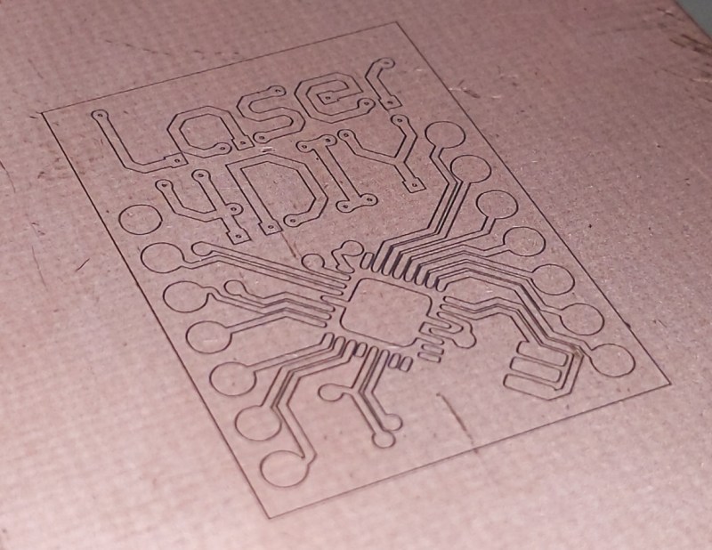
The problem with cutting copper is that it reflects infra-red, so a higher-wavelength blue green laser is used instead. And because you want to ablate the copper, but not melt the surrounding areas or cut straight through the board, extremely short, high-power pulses are the way to go. Here, the [Munich Fab Lab] is using 9 kW pulses of around 30 microseconds each. With these specifications the copper is ablated from the surface of the board allowing for fine details in the range of about 20 µm, which is fine enough for just about any circuit board. The design of the laser head itself is worth a look.
Aside from the laser, the rest is standard CNC machine fodder, but with an emphasis on safety that’s appropriate for a tool in a shared workspace, and the whole project is published under an open license and offers an affordable solution for larger-scale PCB production with extremely fine resolution and without the need for any amounts of chemicals for the more common PCB production methods. There is a lot more information available on the project’s webpage and its GitHub page as well.
Of course, there are other methods of producing PCBs by laser if you happen to have a 20 W fiber laser just kicking around.


Who doesn’t have a 9KW laser laying around the lair?
Oh wait, they are mounted on my pet sharks
It´s of course a Q-switched laser (with a 60W source)
Who doesn’t _want_ to have a 9 kW laser lying around the house?
This is an expensive build, but it’s half as expensive as trying to do it with a fiber laser, and a bunch more in-depth, so that’s cool by me.
Doesn’t this require a license?
Lasers are dangerous in the hands of laymen.
And even more so in the hands of experts. 😆
My father once managed to wield a razor blade with one.
Seriously, though, it would be much safer to just use a photosensitive PCB and an normal laser engraving machine.
If run a few times, the outcome is nice, even with low power.
It also won’t create CU²O that way.
Never take a razor blade to a laser fight.
Nope. No license required, unless you’re selling stuff or performing in public. At least in the US.
And this project really, really handles the safety aspects very well, IMO.
Can’t wait for the FCC to open up the 600 THz band for Hams, so much potential.
https://de-m-wikipedia-org.translate.goog/wiki/Laserschutzbeauftragter?_x_tr_sl=de&_x_tr_tl=en&_x_tr_hl=en&_x_tr_pto=wapp
Thanks Elliot!
When running such lasers openly you certainly have to take some precautions (e.g. safety googles) and there are also some legal requirements, at least in a company context (here in Germany/EU). But the finished device is designed to be fully safe and is prepared to have CE and class 1 laser certification. To fulfill the requirements, it has an light tight metal enclosure, and a safety circuit including redundant switches and a safety relay.
Germans are rules crazy!
I not only got yelled at for walking across the road against the light, I got yelled at for coming back to wait for the light with them.
Reasonably drunk, 3AM, in Berlin, with a km of visibility either way and no cars coming.
Like the man said on the BBC: ‘Germans do as we’re told. Lately we’ve been told to be nice to people. If we were told to open death camps in Poland, we’d do that too.’
My late dad was German. Growing up, I knew he was RULES CRAZY. As an adult, having visited Germany many times, I know he was super relaxed, for a German.
You know the Chine Export (CE) is much easier to get vs the Euro CE cert?
Compliance help from the sane side of the pond.
Rules are made to be broken.
No licenses are needed for lasers. They are regulated by the FDA in the USA and there are rules on how machines are built commercially and implemented. But for a home machine, that’s up to the builder.
Oi mate you got a loicense for dat
Yeah, silly me. I shouldn’t have asked. 😅
I mean, most visitors here are seemingly from the States, after all. That land were people on the run can buy guns and explosives freely without the need to show any ID card, even. Makes me wonder why they have something like the FCC, at all. 😉
I wish we were as cool as you think we are.
True dat!
Uncle Charlie (the FCC) is fully neutered.
Unless you step on aviation or military bands, then you want to _not_get_caught_.
Anything else, go for it. Nobody cares. If you get a HAM license, then they might send you a letter. Best not to get the license, then you’re home free.
The laser wavelength is 532 nm which makes it a green laser.
Exactly. I don’t know where the “blue” comes from.
Yes, it’s green. Also, the pulses are just 2.5ns long (not micro seconds) and the peak power is almost 50kW.
Normally I’d be the last one to criticise something like this – I love lasers, optics, electromechanical stuff – but I have to say, why?
HaD saying “The problem with cutting copper is that it reflects infra-red” is not entirely correct. Define “infra-red”. Yes, copper will happily reflect CO2 laser wavelengths (10.6um) and you’ll never mark copper with it. But a 1064nm fiber laser, which is still infrared, will happily mark copper no problem.
I have a couple of fiber galvo systems (Q-switched fiber-coupled laser source plus a 2-axis mirror galvo and f-theta lens). One is 30W, the other 60W. Both will do great PCBs (e.g. https://imgur.com/a/RA3bsXg). It’s a bad idea to try and ablate all the copper away, because you end up charring the FR4 underneath. The best is to laser off maybe 90% of the copper, then do a quick etch to remove the rest. Gives very nice results.
Big problem with their system is it can only ablate lines as wide as the laser, so for any larger clearances you need to scan an area repeatedly. Doing this with a mechanical X-Y table will take an age. A galvo system is much faster.
And as for “a functional, relatively affordable (around 2000-3000 Euro/USD), and safe machine…..”, I’ve got news for you – for that price, you can buy a complete entry-level fiber laser/galvo system which will do far more than this ever will.
If you’re looking at this as an excercise in building a laser source, fantastic, and it’s something I would loved to have done at one point. But if you’re looking for a way to make PCBs, get a fiber laser. Plus you’ll be able to do a lot else besides.
I would love to know where I can find those 3k euro lasers and also what is that “else” they can do?
Just a newbie who love lasers and know almost nothing about them. So, also any good read about them for “retards” is most welcome. Thanks!
Any lasers I could find are “price on request” and those prices are “ahhh, don’t ask”. :)
If you’re talking about a q-switched fibre laser in the neighborhood of 20W, they actually make PCBs just fine (and can drill holes in FR-4 too.) There is a myth that the blackened FR-4 left behind by cutting with such a laser is conductive. This is not the case, see more here: https://www.bryce.pw/engraver.html
Hi – for some reason I couldn’t reply directly to your comment with some links, so I’ve stuck them down the bottom as a new comment instead!
Based on some videos I’ve seen, when rastering out a larger area of PCB copper, overheating will also become a large problem and the FR4 underneath easily gets burned into conductive carbon.
I have a couple bright copper bars that were engraved by a late 60’s early 70’s (?) 1meter flowing CO2 gas laser (somewhere in the 50-100W range) from Coherent Radiation by a guy that was using it in the early 2000’s to etch wood, glass, plastic, steel, and a few copper things. While I’m sure it lost a significant amt of power to reflection, everything works better with more power right? :-) But yeah, there are better ways to make boards I think…
The laser was awesome though, power supply was 3′ x 2′ x 2′, giant HV xfmr, 2 – 10″ or 12″ tall tubes used for switching beam on/off controlled by a small HeNe guide laser scanned across artwork by slow xy table, very cool to get a good look at it at the time!
CO2 can cut copper, its not as easy as other materials but it can be done. And at work we build machines for drilling microvias in PCBs using CO2 lasers, we can drill up to 9000 vias per second.
Could you please link to some of those entry-level fiber laser/galvo machines?
Sorry, I couldn’t reply directly to you for some reason. I’ve added a comment way down the bottom with some links in it.
Yes, fiber laser have come a long way since we started this project. But one of the most important goals was to build an open hardware device, so comparing it to off-the-shelf, closed systems is a bit unfair. And for that price-point I have not seen a system with a safety enclosure, which was another important topic for us.
But true, fiber lasers are awesome and versatile. Maybe we should build an open hardware fiber laser next?
I sort of get the idea about making this open hardware, but at the end of the day do you really care? Does it really matter that you can build a laser _completely_ from scratch, and have to worry about a whole slew of problems like optical alignment, sourcing just the right sort of laser crystal, temperature control, driving the pump diode etc. etc.? It all depends what sort of “level” you want it to be “open hardware” at.
Take a typical fiber laser galvo system from China, like the two I’ve got. If so desired, I could drive the laser module directly and have full control over power, pulsewidth, frequency etc. – this is all clearly documented in the manual. I don’t care about the finer intricacies of how a master-oscillator-power-amplifier laser works, it’s not relevant. Similarly, I could drive the galvo head directly as well (indeed, I’m working on an add-on that does this) – the protocol is very simple and widely documented (basically clock + data for both axes, over a differential pair link). I don’t care about PID loops, tuning, and all the stuff that goes on inside the galvo itself.
My point: I can buy a 20W Raycus fiber laser source for £500 and get on with doing cool shit with it. Why would I want to build one from scratch?
The open source laser this team developed is really cool. It may not be the cheapest or best tool for PCb , but open source has never been about that….Mac may have a lot of advantages over my Linux box, but I will stick to Linux cause I can fix it, and am not vendor locked, and/or I like to hack stuff. This tool may be serviceable way after the China laser is dead…or hope it will lead to better designs in future
I am able to cut PCBs on a 1064 nm, 20W, q-switched fibre laser without issue. The real trick is overcoming imperfections in the f-theta lens / calibration (which of course you can do by going without an f-theta lens and using a cartesian robot — though the f-theta does let you scan extremely fast and doing many light passes rather than trying to blast through the copper in one go is thermally advantageous given the inefficiency of cutting with 1064nm.)
Worth noting that while copper reflects 1064nm fairly well, plasma does not.
i love the idea of yet another way to etch boards but doesn’t this perform vapor deposition of copper onto your workspace? anyways it terrifies me, and i’m even someone who uses a bench grinder in the same room as my 3d printer and electronics workbench :)
Copper is toxic to quite a few people, and vaporizing it seems like a pretty bad idea.
You should have a fume extractor when doing metal ablation, and the Laser4DIY device has fume extraction.
This laser is only DIY as far as you can get parts for the laser source! Unless you have an in with some university or laser component supplier, the parts needed to construct the source would classify as quite exotic. A single chip solid state laser crystal with reflectors and a passive q switch already bonded on is not easy to get, nor are some of the other components needed to build this. A fiber laser is way easier to acquire and use for DIY, even if you have to use galvos and an f-theta lens. That kind of build would be a lot easier to duplicate. Lastly If you need to do anything using AC line voltages on your PCB, you wouldn’t want to use this to do the ‘etching’ as any carbonization of the FR4/Substrate will cause it to be way more conductive than it should be, as well as taking a very long time to ‘etch’ if you happen to need larger spacing between conductive areas. I can hear the conversation now, “Hey, I have this cool solid state laser chip and some other parts they surplused out from the laser lab at my university, what should we build with it?…” Neat machine, but as far as being easy for others to duplicate, this one appears to be a one off. Kudos for the Open Source docs, but sadly, I don’t see a lot of possibility for most to be able to duplicate this build.
Buying a laser is not the DIY we had in mind. We wanted a real open hardware solution, where you (can) build the laser source yourself. Granted, the laser crystal is nothing you can buy on ebay, but you can source it! We are not a university or company and were able to get these parts directly from Asian manufacturers. Single quantities are expensive, but we might organize a group buy if there are interested people.
The magic here is the cute little pulsed green laser they made. Fascinating stuff if you dig into the site. An 808 nm diode laser optically pumps (shines on) a Nd doped YAG crystal (very common) which then lases at 1064 nm or whatever, which then goes out to hit a KTP crystal, which at high enough power does weird stuff, like generate a second harmonic, AKA doubles the frequency, AKA makes the IR green. Oh also I think they said they Q-switched the main 1064 laser, which makes sense with that beefy pulse. That’s basically when they only let the resonator mirrors do their work after the laser has had a good long time to pump up the active material. Think of it kinda like charging up a capacitor and discharging all at once. Same-ish average power, but savage instantaneous wattage during those pulses.
And no you can’t just take a crystal of KTP and look through it and see IR turned to green – it needs that crazy power to generate those “non-linear optical” effects. And some people have made lasers that generate a third harmonic too, but they’re not common. Probably others beyond that.
So why don’t they just double the 808 diode light? Slip the YAG laser? Because the beam quality of diodes suck and anyways their instantaneous power isn’t enough to set the KTP to doubling. The little green pointers we used to have the KTP crystal WITHIN the resonant cavity of the YAG laser, so the circulating power is enough to double. But continuous.
Major rabbit hole here, I’m sure I got a few things wrong too. Lasers are awesome.
Great work. Don’t forget to filter out the IR from your output beam… Are you sure you’re not cutting the copper with 1064nm AND 532nm?
Chinese laser pointer makers were famous for leaving out IR filters. Sent power readings off the charts!
NdYag crystals are common, The ‘Microchip’ laser they talk about, however, is a specialized bonded crystal assembly, that you might get lucky maybe and score one on ebay if you are always trolling for that kind of stuff, though the condition would be suspect, as most of the stuff you find on ebay, especially YAG crystals, are surplus because they have some kind of defect.
“Major rabbit hole here, I’m sure I got a few things wrong too. Lasers are awesome.”
Actually, I enjoyed reading these lines. Thanks! 🙂
Laser beam quality is something I often worry about, too.
I find real gas/valve lasers to have a nicer beam than the usual diode lasers (HeNe vs laser diode+resonator crystal).
It’s related to coherence and other factors, I suppose. Not sure how to explain.
The gas laser has that laser-like sparkle and fine, bright beam, while the diode laser needs adjustment optics (huh?) and looks generally wishy-washy.
I’m more into holography and communications, though.
Maybe that’s why I have weird opinions here. 😂
The 808 is mostly only good for pumping. The high power is crap quality wise and there are other issues.
We use THG lasers at work for our flex PCB machines, there are quite a few of these lasers out there. I know we have messed around with 4HG and I think 5HG but the optics start getting expensive and its much harder to work with the beam. At 343 or 355 your still working in the range that cameras can see the beam to do stuff like collimation. Once you get to 266 things get tricky.
They will have some 1064 mixed in unless they put a 532 pass filter on it. They could use the 1064/532 mix to get 355 through another crystal.
Hi Andy, thanks!
You explained the laser nicely!
Concerning IR: The last 2 mirrors in the setup have a HR@532nm coating and transmit only approx. 50% of the power at 1064 nm, which is therefore not relevant for the later ablation process
This looks like WAY overkill to me, especially for a DIY PC board. I simply spray paint a copper clad board with cheap flat black spray paint, laser etch the paint to remove it using a $200 desktop laser engraver, and then etch the copper with ferric chloride. The resolution is limited by the copper etch, not the paint.
This is the way. Cheap, easy and great resolution. I have etched very fine boards with a $200 eleks laser
Sourcing and disposing of chemicals is annoying.
Test comment….
So, which characteristics of your comment would you like us to test?
B^)
:-) I was trying to reply to an individual comment, with some links, above, but it refused to post for some reason! I stuck it down as an extra comment instead….
DIY Laser For Ablating
MetalHot DogsHuh. For some reason I can’t reply to individual comments. Anyways, for those wondering about fiber engravers –
Cloudray are one that list an actual price:
https://www.cloudraylaser.com/collections/qs-series/products/qs-30-litemarker-30w-split-laser-engraver-fiber-marking-machine-with-4-3-x-4-3-7-9-x-7-9-working-area
However you’re usually better talking to an actual manufacturer and getting a specific quote (I know, I usually get annoyed by that sort of thing, but the times I’ve done it they’ve been very helpful). Three which are frequently mentioned:
https://www.omglaser.com/products/fiber-laser-engraving-machine/
https://www.bogongcnc.com/fiber-laser-marking-machine/mini-fiber-laser-marking-machine.html
http://www.bwmtech.cn/index.php/product/index/g/e/id/5.html
No affiliation, but I have bought lasers from both Bogong and BWM and been very happy with them.
Also see the two main Facebook groups for fiber lasers:
https://www.facebook.com/groups/fiberlasers
https://www.facebook.com/groups/fiberlaserthenextlevel
“higher wavelength”?