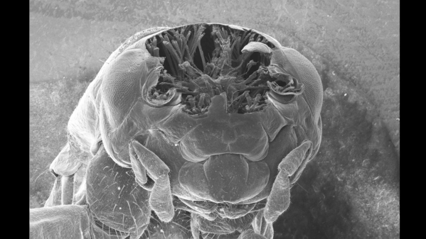
A scanning-electron micrograph is shown of a cricket's body, focusing on the head, which has been sliced off just above the eyes.

Cross-Sectioning Crickets With A Femtosecond Laser

Unlike most cutting lasers, femtosecond lasers don’t vaporize materials; rather, they produce such short, intense bursts of light that the affected region is ablated without having the chance to heat its surroundings. This makes them good at cutting away material without damaging the surroundings, something [Ben Krasnow] exploited to cut cross-sections of samples while still in a scanning-electron microscope.

In this case, the samples were crickets, and before imaging they had to be prepared. First, the bodies were soaked in glutaraldehyde to cross-link the proteins and stabilize the structure. Next, a series of solvent exchanges replaced the water in the bodies with a low-surface-tension solvent; this meant that during the next step, drying, surface tension wouldn’t distort the crickets’ internal structure. Finally, the insect bodies were charred under argon, which made the bodies conductive and more absorptive to laser light.

The laser itself and the scanning galvo are mounted outside the microscope, and shine in through a transparent window. To protect the detector and electron optics from a spray of ablated carbon, a servo motor swings an aluminium shutter between these and the sample while the laser is active. This caused some mysterious problems during testing: after the first ablation run, the electron microscope’s image would contain so much noise as to be unusable, but it would improve over time. As it turned out, the shutter was painted, and the other side of the paint was getting coated with charged carbon particles. This created a small capacitor which disrupted the electron optics as it discharged. Eventually, after solving this and a few other strange problems, [Ben] was able to take several time-lapse videos of the laser gradually ablating a cricket, 30 microns at a time, revealing its inner structure.

Although scanning-electron microscopes are unfortunately shard to come by, it’s still possible to restore a secondhand microscope or, as [Ben] did, build your own. Femtosecond lasers are yet more inaccessible, though they can be used to replicate themselves.

Continue reading “Cross-Sectioning Crickets With A Femtosecond Laser”
Laser Fault Injection, Now With Optional Decapping

Whether the goal is reverse engineering, black hat exploitation, or just simple curiosity, getting inside the packages that protect integrated circuits has long been the Holy Grail of hacking. It isn’t easy, though; those inscrutable black epoxy blobs don’t give up their secrets easily, with most decapping methods being some combination of toxic and dangerous. Isn’t there something better than acid baths and spinning bits of tungsten carbide?

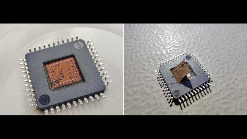
[Janne] over at Fraktal thinks so, and the answer he came up with is laser decapping. Specifically, this is an extension of the laser fault injection setup we recently covered, which uses a galvanometer-scanned IR laser to induce glitches in decapped microcontrollers to get past whatever security may be baked into the silicon. The current article continues that work and begins with a long and thorough review of various IC packaging technologies, including the important anatomical differences. There’s also a great review of the pros and cons of many decapping methods, covering everything from the chemical decomposition of epoxy resins to thermal methods. That’s followed by specific instructions on using the LFI rig to gradually ablate the epoxy and expose the die, which is then ready to reveal its secrets.

The benefit of leveraging the LFI rig for decapping is obvious — it’s an all-in-one tool for gaining access and executing fault injection. The usual caveats apply, of course, especially concerning safety; you’ll obviously want to avoid breathing the vaporized epoxy and remember that lasers and retinas don’t mix. But with due diligence, having a single low-cost tool to explore the innards of chips seems like a big win to us.

DIY Laser For Ablating Metal

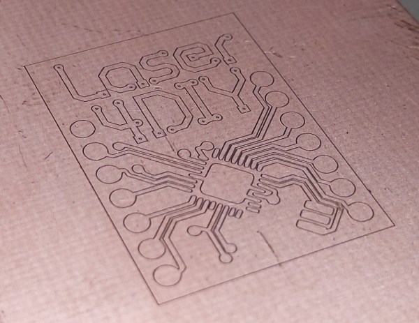
For those who wish to go beyond through-hole construction on perfboard for their circuit boards, a printed circuit board is usually the next step up. Allowing for things like surface-mount components, multi-layer boards, and a wider array of parts, they are much more versatile but do have a slight downside in that they are a little bit harder to make. There are lots of methods for producing them at home or makerspace, though, and although we’ve seen plenty of methods for their production like toner transfer, photoresist, and CNC milling, it’s also possible to make them using laser ablation, although you do need a special laser to get this job done.

The problem with cutting copper is that it reflects infra-red, so a higher-wavelength blue green laser is used instead. And because you want to ablate the copper, but not melt the surrounding areas or cut straight through the board, extremely short, high-power pulses are the way to go. Here, the [Munich Fab Lab] is using 9 kW pulses of around 30 microseconds each.  With these specifications the copper is ablated from the surface of the board allowing for fine details in the range of about 20 µm, which is fine enough for just about any circuit board. The design of the laser head itself is worth a look.

Aside from the laser, the rest is standard CNC machine fodder, but with an emphasis on safety that’s appropriate for a tool in a shared workspace, and the whole project is published under an open license and offers an affordable solution for larger-scale PCB production with extremely fine resolution and without the need for any amounts of chemicals for the more common PCB production methods. There is a lot more information available on the project’s webpage and its GitHub page as well.

Of course, there are other methods of producing PCBs by laser if you happen to have a 20 W fiber laser just kicking around.