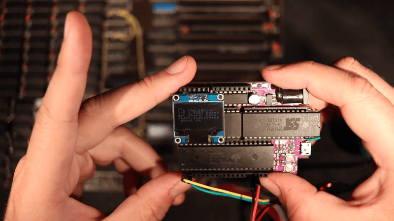
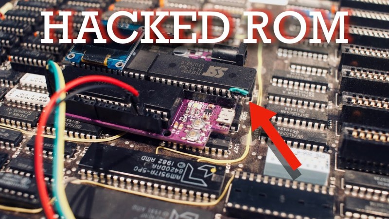
What’s the difference between a 64k ROM in a 28-pin DIP and a 128k ROM in a 32-pin DIP? Aside from the obvious answers of “64k” and “four pins,” it turns out that these two chips have a lot in common, enough so that it only takes a little bodging to make them interchangeable — more or less.
For a variety of reasons revealed in the video below, [Anders Nielsen] use the SST39SF010, a Flash ROM in a 32-pin DIP, in place of the old standby W27C512, an EEPROM in a 28-pin DIP. To deal with those pesky extra pins on the Flash ROM, [Anders] dug into the data sheets and found that thanks to JEDEC standards, almost everything about the pinouts of the two chips is identical. The only real difference is the location of Vcc, plus the presence of a 16th address bus line on the more capacious Flash ROM.
Willing to sacrifice the upper half of the Flash chip’s capacity, [Anders] set about bodging the 32-pin chip to work in a 28-pin socket. The mods include a jumper from pin 32 to pin 30 on the Flash chip, which puts Vcc in the right place, and adding a couple of pull-up resistors for write-enable and A16. Easy enough changes, but unfortunately, [Anders] chose a Flash ROM with heavily oxidized pins, leading to some cold solder joints and intermittent problems while testing. There’s also the fact that not all boards have room for overhanging pins, a problem solved by adding a socket to create a little vertical clearance.
We found this to be a neat little hack, one that should make it a bit easier to use the wrong chip for the job. If you want to see where [Anders] is using these chips, check out his 6502 in an Arduino footprint or the bring-up of an old XT motherboard.


Maybe it’s time to break away from the Arduino footprint and design a proper PCB.
this, so much. Altho I like the many shields I got and the arduino’s and clones. there is little use to keep on making them in this form factor. the Pi Pico already did a better job.
I only use breadboardable arduinos… like the nano
It was time to step away the second they started making them.
The pinouts are designed so you can do this…drop a larger chip into the footprint of a smaller one. The pin count does, of course, increase after you get past a certain number of address bits.
You might even expect me to dive into why that is in the video ;-) … @2:45
Sorry. Not trying to be snarky. I designed with these things, back in te age of DIPs and UV erasure, so it’s obvious to me.
Thanks for the nice writeup! Always too kind to the not so high tech hacks :)
I had a feeling some of the retrocrowd were having issues finding the right BIOS ROM for whatever board, so I made this quick video to show it’s not that hard to make the conversion if you can only source the still-in-production DIPs.
Re: Arduino footprint for the 65uino – good luck stuffing a DIP 6502 + support IC’s into a Pi Pico form factor. Or a DIP zif socket for that matter :D
Considering it’s meant to be an exercise in DIP recycling, assembly code basics, and extreme constraint, while still ending up with a really useful tool, I think the Arduino footprint is a great choice for the 65uino project – for the less constrained projects I already have my ABN6502 SBC R1.
Besides – ST is still selling plenty of Nucleo boards, that might be a better place to start phasing out the footprint.
You don’t need a special footprint. Just lay out the PCB according to the components you use. Why this is even worth an article, I honestly can’t understand. On the other hand, I have submitted three tips in the last few days, all of which have been ignored.
If you can’t say something nice….
This is a perfect example of a hack. In the real world, you don’t always have the exact part you need, when you need it – but if you find something close enough, you can finesse it into service.
This is also an important reminder for anyone who designs PCBs for a living: if there are multiple suitable parts, design to the largest/worst case, and bake in multiple assemblies to keep from having to spin the board if a single part is unavailable.
Some people confuse hacking with messing up. Some people see constructive criticism as a personal insult.
Your implication seems to be that the article is not worth the writeup… I disagree. It was also not a mess-up.. a fact that is plainly evident if you care to watch the video.
The point of constructive criticism is to improve the quality of information, not cut others down because HaD chose this article over the ones you offered. If you honesly intended your comment to be constructive… I would ask you to solicit feedback from those closest to you regarding the quality of your criticism, because you missed the mark.
TL:DR – Anders, good work, and thank you for sharing. MelB, don’t be such a grouch.
“Some people confuse hacking with messing up.”
Just FYI, that comment comes across as an insult. It also makes you look like you don’t know what you are talking about.
“Some people see constructive criticism as a personal insult.”
I don’t see anything in your original post that could be considered constructive or useful.
But since you like constructive criticism so much: Try to avoid making your comments so abrasive, this will make interactions with you more valuable, also it will increase the likely hood that people will take you seriously and consider your contributions to have value.
Perhaps the reason your submissions didn’t get picked up is due to your communication style rather than the quality of your tips?
Because most of the time this trick if used on existing boards, not boards you design and knows in advance you would use it with 32-pin memory chips.
“On the other hand, I have submitted three tips in the last few days, all of which have been ignored.”
Yeah ? Were they hacks ? Like this one, this is a hack, making use of what you’ve got to do what you want.
The pin hack is very well known in some parts of the retro community, for instance, fitting standard 28 pin UV-EEPROMs into the 24 pin sockets on your C64 by sandwitching two DIP sockets with some pins bent, like this:
http://dusted.dk/pages/c64/MaxFake64/pic/ROMadapterl.jpg
http://dusted.dk/pages/c64/MaxFake64/pic/ROMadapter2l.jpg
You could design a small daughter board for bigger ROM chip and use wire posts (not goldpins as they are too thick for sockets) to plug it into original ROM socket. With some dip switches for the additional address lines you can get 4 ROM variants on one chip. I encountered this way of making chip replacement boards when disassembling a broken third party 5,25″ FDD drive for Atari 8-bit computers some 20 years ago.
On related note I really, really hate Arduino footprint, which was a result of incompetence and laziness of the designer.
Back in the 1980’s I did this when converting from 28 pin EPROMs to 24 pin EPROMs, mostly for switching versions on C64 ROMs (236427128/27256).
I’ve used two socket, one 24 pins and one 28 pins and did all the pinout adaptation on the socket tower itself, keeping both the C64 and the new EPROM unmodified.
Neat trick :) I thought about this but the value proposition hasn’t aged very well. If you look up sockets on Farnell and compare them to the 1$ of the used ROM it’s a strange world.
The beauty of modifying the ROM like this is that it’s essentially electrically unmodified afterwards.
Other than price, the main difference was that back then we had to work with EPROMs, and the 15-20 minute erase cycle on the UV lamp required us to use several EPROMs for development, since we did not want to wait for them to get cleared.
In addition, I always used a larger ROM with a switch so I could always move back to the original version. This is harder and more cumbersome to do on the chip itself.
Another similar thing I also did years ago was to create a DiskOnChip 2000 programmer out of the ROM socket of an ST-02 ISA disk controller:
http://web.archive.org/web/20090829232859/http://geocities.com/SiliconValley/Campus/3216/doc2000/st02doc2000.htm
Reminds me of a hack of the 90s.
The BBS version (TNN or XNet?) of “The Firmware” (TF), a popular AX.25 software for TNCs in Europe, was using back-switching.
It used a spare pin of one of the i/o ICs or the Z80 to address more memory..
Or rather, to pull an EPROM pin high/low..
Aka bank switch.
Sorry for the typo. The auto-correction feature always knows better and gets in the way. 😔
By programming the same data in the upper and lower half, then A16 becomes a don’t care — can tie to GND, VDD, or A15 etc. You’ll get the same output.
Exactly, that’s the scriptable solution. I kinda mention that in the video – and it’s also in the last link in Dan’s writeup (about my XT).
What is it with all the snarky comments on the HAD posts these days?
Articles like this are the bread and butter of this site… it’s a hack for goodness sake!
Yes, chips have advanced, SMD is more prevalent, you COULD use more modern chips, a different form-factor for your board or a different layout.
To me, it’s all about learning. Everything is not set in stone. There’s no one right way to do things. “Messing up” is part of the process of learning.
I can see this being especially useful for repairs to things such as retro arcade boards where the EEPROM/Flash chips might be unobtanium.
These are the kinds of posts that make this site so interesting.
Thanks to Anders and Dan for the article. Ignore the idiots.
Learning results in improvement. From an engineering point of view, there is of course a way to do things right. Protruding pins are definitely not one of them, if only because of the risk of injury. A better solution would be to design a carrier pcb, for example. The best solution, however, would be to drop the Arduino PCB design and redesign it from scratch. My posts may seem harsh and insulting, but that may be due to my illness (bipolar disorder), I stopped apologizing for it a long time ago.
You go ahead and redesign the IBM XT motherboard in the video for 32 pin ROMs if you think that’s the best solution.
No worries :)
A better hack would be modifying the thing the larger capacity chip is plugged into to use 128K.
Or providing a switch to switch between using the upper and lower halves of the chip, that way you could have two different sets of code that are easy to switch between.