Book8088 Slows Down To Join The Demoscene

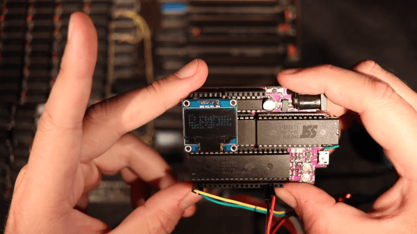
As obsolete as the original IBM Model 5150 PC may appear, it’s pretty much the proverbial giant’s shoulders upon which we all stand today. That makes the machine worth celebrating, so much so that we now have machines like the Book8088, a diminutive clamshell-style machine made from period-correct PC chips; sort of a “netbook that never was.”

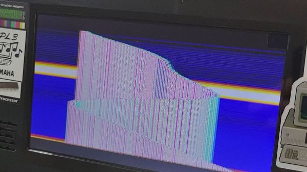
But the Book8088 only approximates the original specs of the IBM PC, making some clever hardware hacks necessary to run some of the more specialized software that has since been developed to really stretch the limits of the architecture. [GloriousCow]’s first steps were to replace the Book8088’s CPU, an NEC V20, with an actual 8088, and the display controller with a CGA-accurate Motorola MC6845. Neither of these quite did the trick, though, at least not on the demanding 8088MPH demo, which makes assumptions about CPU speed based on the quirky DRAM refresh scheme used in the original IBM PC.

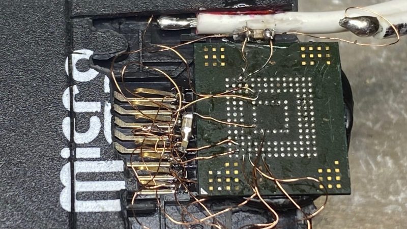
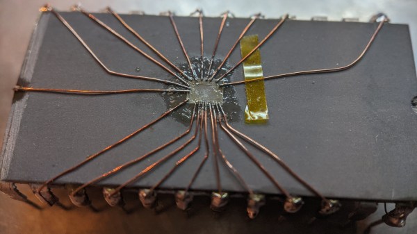
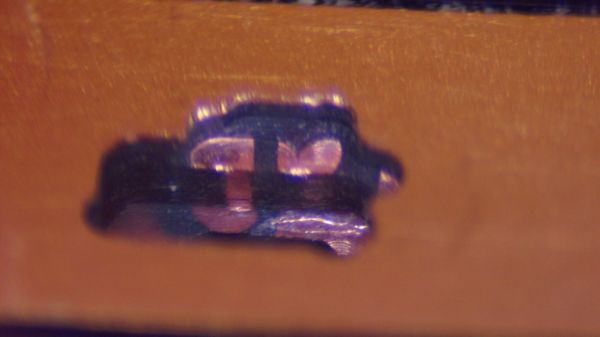
Knowing this, [GloriousCow] embarked on a bodge-fest aimed at convincing the demo that the slightly overclocked Book8088 was really just a 4.77-MHz machine with a CGA adapter. This involved cutting a trace on the DMA controller and reconnecting it to the machine’s PIO timer chip, with the help of a 74LS74 flip-flop, a chip that made an appearance in the 5150 but was omitted from the Book8088. Thankfully, the netbook has plenty of room for these mods, and with the addition of a little bit of assembly code, the netbook was able to convince 8088MPH that it was running on the correct hardware.

We thoroughly enjoyed this trip down the DMA/DRAM rabbit hole. The work isn’t finished yet, though — the throttled netbook still won’t run the Area 5150 demo yet. Given [GloriousCow]’s recent Rust-based cycle-accurate PC emulation, we feel pretty good that this will come to pass soon enough.

Stuffing A 32-Pin Chip Into A 28-Pin Socket

What’s the difference between a 64k ROM in a 28-pin DIP and a 128k ROM in a 32-pin DIP? Aside from the obvious answers of “64k” and “four pins,” it turns out that these two chips have a lot in common, enough so that it only takes a little bodging to make them interchangeable — more or less.

For a variety of reasons revealed in the video below, [Anders Nielsen] use the SST39SF010, a Flash ROM in a 32-pin DIP, in place of the old standby W27C512, an EEPROM in a 28-pin DIP. To deal with those pesky extra pins on the Flash ROM, [Anders] dug into the data sheets and found that thanks to JEDEC standards, almost everything about the pinouts of the two chips is identical. The only real difference is the location of Vcc, plus the presence of a 16th address bus line on the more capacious Flash ROM.

Willing to sacrifice the upper half of the Flash chip’s capacity, [Anders] set about bodging the 32-pin chip to work in a 28-pin socket. The mods include a jumper from pin 32 to pin 30 on the Flash chip, which puts Vcc in the right place, and adding a couple of pull-up resistors for write-enable and A16. Easy enough changes, but unfortunately, [Anders] chose a Flash ROM with heavily oxidized pins, leading to some cold solder joints and intermittent problems while testing. There’s also the fact that not all boards have room for overhanging pins, a problem solved by adding a socket to create a little vertical clearance.

We found this to be a neat little hack, one that should make it a bit easier to use the wrong chip for the job. If you want to see where [Anders] is using these chips, check out his 6502 in an Arduino footprint or the bring-up of an old XT motherboard.

Continue reading “Stuffing A 32-Pin Chip Into A 28-Pin Socket”

Dumping An EMMC Chip With Many Bodge Wires

Sometimes, you know where the data you need is stored, you just don’t have a way to access it. In this case, [GetHypoxic] needed to rip data off an eMMC chip, salvaged out of a camera. With no desire to wait for an adapter to show up, it was time to bust out the bodge!

Once removed from the PCB, bodge wires were attached to the ball-grid array contacts on the bottom of the chip. Incredibly fine soldering was the order of the day to get these hooked up to the tiny pads, and we count 11 or 12 bodge wires in total. 1.8 volts was manually supplied to the eMMC chip, and it was directly wired up to the contacts of a built-in card reader out of an old laptop for reading.

Despite the rats-nest look of it all, and the yellow polyimide tape holding it together, [GetHypoxic] reported that it mounted successfully and got the job done. We’ve seen similar hacks before, too, wiring eMMC chips up to SD card adapters. It might look messy, but hey – it sure beats waiting for shipping!

The decapped chip on top of some other DIP IC, with magnet wire soldered to the die, other ends of the magnet wire soldered to pins of the "body donor" DIP IC.

Factory Defect IC Revived With Sandpaper And Microsoldering

We might be amidst a chip shortage, but if you enjoy reverse-engineering, there’s never a shortage of intriguing old chips to dig into – and the 2513N 5×7 character ROM is one such chip. Amidst a long thread probing a few of these (Twitter, ThreadReader link), [TubeTime] has realized that two address lines were shorted inside of the package. A Twitter dopamine-fueled quest for truth has led him to try his hand at making the chip work anyway. Trying to clear the short with an external PSU led to a bond wire popping instead, as evidenced by the ESD diode connection disappearing.

A dozen minutes of sandpaper work resulted in the bare die exposed, making quick work of the bond wires as a side effect. Apparently, having the bond pads a bit too close has resulted in a factory defect where two of the pads merged together. No wonder the PSU wouldn’t take that on! Some X-acto work later, the short was cleared. But without the bond wires, how would [TubeTime] connect to it? This is where the work pictured comes in. Soldering to the remains of the bond wires has proven to be fruitful, reviving the chip enough to continue investigating, even if, it appears, it was never functional to begin with. The thread continued on with comparing ROMs from a few different chips [TubeTime] had on hand and inferences on what could’ve happened that led to this IC going out in the wild.

Such soldering experiments are always fun to try and pull off! We rarely see soldering on such a small scale, as thankfully, it’s not always needed, but it’s a joy to witness when someone does IC or PCB microsurgery to fix factory defects that render our devices inoperable before they were even shipped. Each time that a fellow hacker dares to grind the IC epoxy layers down and save a game console or an unidentified complex board, the world gets a little brighter. And if you aren’t forced to do it for repair reasons, you can always try it in an attempt to build the smallest NES in existence!

Continue reading “Factory Defect IC Revived With Sandpaper And Microsoldering”

PCB internal bodge

PCB Microsurgery Puts The Bodges Inside The Board

We all make mistakes, and there’s no shame in having to bodge a printed circuit board to fix a mistake. Most of us are content with cutting a trace or two with an Xacto or adding a bit of jumper wire to make the circuit work. Very few of us, however, will decide to literally do our bodges inside the PCB itself.

The story is that [Andrew Zonenberg] was asked to pitch in debugging some incredibly small PCBs for a prototype dev board that plugs directly into a USB jack. The six-layer boards are very dense, with a forest of blind vias. The Twitter thread details the debugging process, which ended up finding a blind via on layer two shorted to a power rail, and another via shorted to ground. It also has some beautiful shots of [Andrew]’s “mechanical tomography” method of visualizing layers by slowly grinding down the surface of the board.

[Andrew] has only tackled one of the bodges at the time of writing, but it has to be seen to be believed. It started with milling away the PCB to get access to the blind via using a ridiculously small end mill. The cavity [Andrew] milled ended up being only about 480 μm by 600 μm and only went partially through a 0.8-mm thick board, but it was enough to resolve the internal short and add an internal bodge to fix a trace that was damaged during milling. The cavity was then filled up with epoxy resin to stabilize the repair.

This kind of debugging and repair skill just boggles the mind. It reminds us a bit of these internal chip-soldering repairs, but taken to another level entirely. We can’t wait to see what the second repair looks like, and whether the prototype for this dev board can be salvaged.

Thanks to [esclear] for the heads up on this one.

Micro-Sized Flex For Commercial Quality Bodging

We love watching the creativity unleashed by the democratization of once-exotic technologies. The casualness by which one can order a cheap, small run of PCBs has unlocked a flood of fine pitch components and projects which look commercial quality even with a total build volume of one. Now the once mythical flex PCB has been falling from it’s stratospheric pricing and with OSHPark’s offering it feels like we’re at the inflection point. [qwertymodo] leveraged this by creating a beautifully twisted flex to add link port support to the Super Game Boy

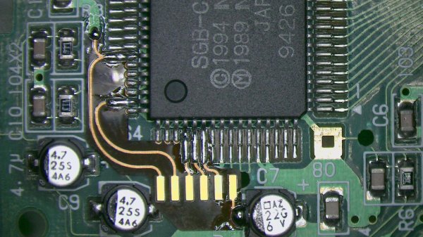
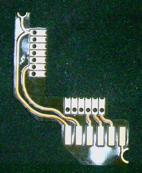
In the mid-90’s Nintendo released the Super Game Boy, a cartridge for the SNES which allowed you to play Game Boy games on the big screen. Each cartridge was in fact an entire Game Boy with the appropriate hardware to present it in a way the host console could interface with, but missing some of the hardware a standalone Game Boy would include like a link port to connect it to another system. This mod fixes this limitation by bridging the correct pins out from the CPU to a breakout board which includes the link port connector. For general background on what’s going on here, check out [Brian]’s article from April describing a different mod [qwertymodo] executed to the same system.

What’s fascinating is how elegant the mod is. Using a a flex here to create a completely custom, strangely shaped, one-of-a-kind adapter for this random IC, in low volume is an awesome example of the use of advanced manufacturing techniques to take our hacks to the next level. It reminds us a little of the method [Scotty] used to add the headphone jack to his iPhone 7 back in 2017. At the time that seemed like a technology only available to hackers who could speak a little Mandarin and lived in Shenzhen.

Detailed information on this hack is a little spread out. There is slightly more info in these tweets, and if you have a Super Game Boy crying out for a link port the adapter flexes are sometimes available here. Look beyond the break to see what the mod originally looked like sans-flex.

Continue reading “Micro-Sized Flex For Commercial Quality Bodging”