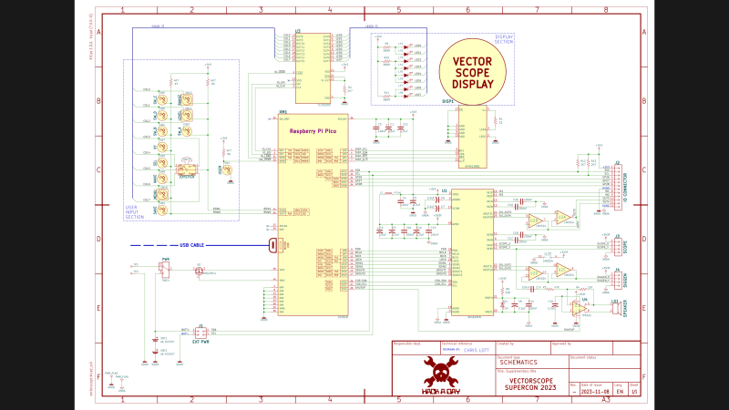
When I saw this year’s Supercon Vectorscope badge, I decided that I had to build one for myself. Since I couldn’t attend in-person, I immediately got the PCBs and parts on order. Noting that the GitHub repository only had the KiCad PCB file and not the associated schematics and project file, I assumed this was because everyone was in a rush during the days leading up to Supercon weekend. I later learned, however, that there really wasn’t a KiCad project — the original design was done in Circuit Maker and the PCB was converted into KiCad. I thought, “how hard can this be?” and decided to try my hand at completing the KiCad project.
Fortunately I didn’t have to start from scratch. The PCB schematics were provided, although only as image files. They are nicely laid out and fortunately don’t suffer the scourge of many schematics these days — “visual net lists” that are neither good schematics nor useful net lists. To the contrary, these schematics, while having a slightly unorthodox top to bottom flow, are an example of good schematic design.
Graphical Lines to PCB Traces
The first thing I took a look at was the features on the PCB file, since I was hoping to extract the net names from the traces. Unfortunately, when I looked at the traces, they were just graphical lines. I knew from previous digging on the KiCad user forums that going backwards from a PCB to a schematic is an unnatural workflow. But I was surprised that there in recent versions of KiCad (I am using v7) there is a feature to convert graphical lines into traces.


One non-obvious quirk to be aware of — this operation duplicates the selected the graphical lines before converting them into traces, resulting overlapping elements. This can be confusing, because the newly-created trace is presented by PCBNEW as being underneath the original graphical line, making it appear that the conversion failed. The solution is to immediately delete the selected items, and the converted tracks will remain. You can do this on an entire board at once by disabling everything except graphical items in the selection filter and just select an entire layer for conversion.
Part Footprints
When designing a PCB, the task of mapping the schematic symbols into their corresponding physical footprints can be tedious. Most modern CAD tools with their corresponding parts management schemes make this process easier than ever, but it can still be a headache when you are using parts not in the libraries. We’re going backwards in this design, so I wasn’t quite sure what problems might exist. But a quick glance at the PCB file shows that the parts on the board are really footprints. This seems promising, so let’s move on to making schematics.
Automatic Schematic Generation?
The usual design flow is from schematics to PCB, whether you’re using a CAD tool or doing everything by hand. Changes to a schematic are reflected on the PCB layout. Modern PCB CAD tools can update a PCB design automatically from the schematics, updating the net list and adding and/or removing parts as needed. These tools even take a stab at placing any new parts for you. Even if this is only a jumbled cluster of footprints, it’s easier than adding each part manually. But can you go the other direction?
There are also long-established processes for going the other direction, from PCB to the schematics, which have been around longer than computerized CAD tools. Perhaps the most common of these is called back annotation. Once the layout is substantially complete, the designer will re-sequence the reference designators on the board so that they appear in some order and are easy to find by people working on the PCB. We often skip this step for the kinds of small boards people make today, but if you’re making a 9U Eurocard design that is some 350 mm square, you really need to re-sequence the reference designators and back annotate the schematic.
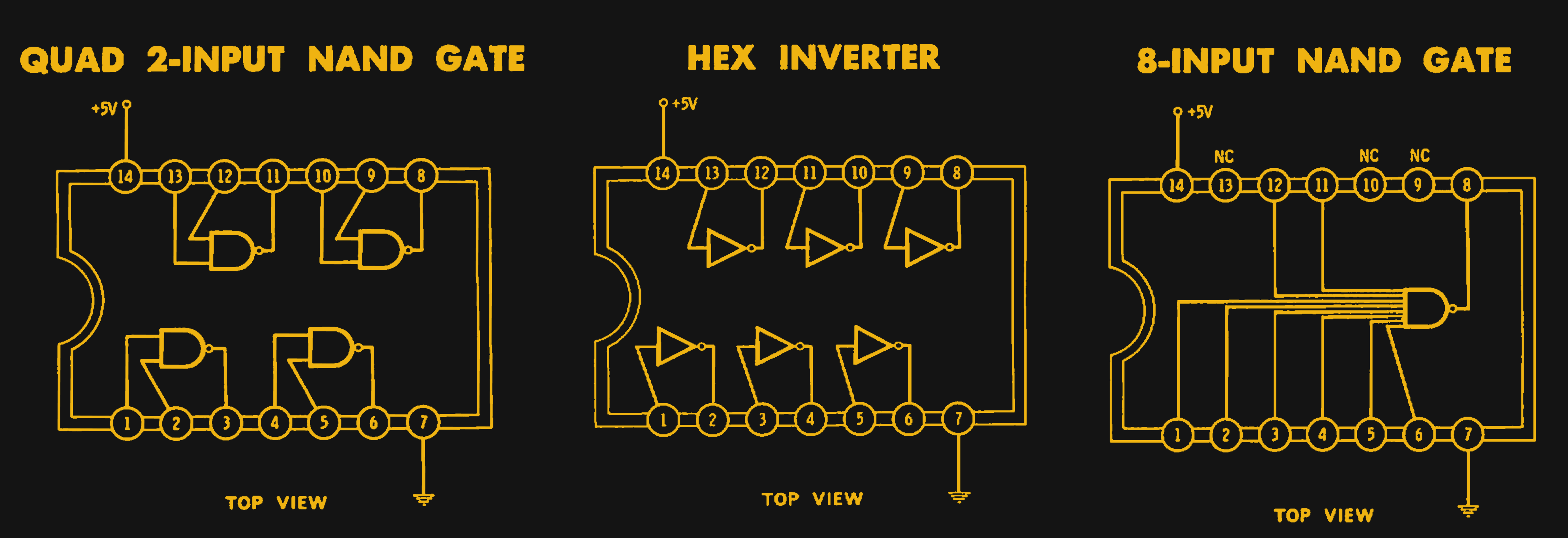
Another example of this backwards flow is gate swapping, so-named because it was very common in old designs using 74-series TTL logic chips. These chips have multiple gates per chip, single logic gates with multiple inputs, or both. Fortunately, CAD tools such as KiCad have provisions for these as well.
But we have the complete opposite of the normal “have a schematic and want to populate a new blank PCB” situation. Can I get KiCad to similarly populate a schematic from an existing PCB, no matter how ugly and disorganized it would be? Conceptually it doesn’t seem far fetched, given the existing KiCad capabilities. But in practice, the answer is no.
Make Schematics
Not unexpectedly, I needed to re-draw these schematics from scratch. Fortunately, this project doesn’t have a lot of parts and many of those parts are standard and found in KiCad or my own libraries. Equipped with the original documentation, I proceeded to draw the schematics in KiCad. Rather than making an exact duplicate of the existing schematics, I decided to rearrange the flow of the circuit into the more familiar left-to-right direction.
I started with just the main chips and components, ignoring connections and discrete components at first. Some of the parts weren’t in my libraries and had to be constructed in the KiCad symbol editor. I normally start with a large schematic sheet, realizing the page can always be resized later if needed ( I guessed A3, which turned out to be correct ). With all the chips on the page, you have to move things around until the visual flow on the page describes the actual logical flow of the design. Similar to placing components on a new PCB layout, there is no clear-cut process to place schematic symbols on a blank page. But here are some general concepts that I’ve learned over the years that I find helpful:
- Take a step back from circuitry, and consider the inputs, outputs, and functionality of the overall design as if it were a black box.
- Flow goes from left to right, inputs on left, outputs on right.
- Connectors go on the sheet edges, or for large designs, put all connectors on page 1.
- Group circuits together by function on the page, or for large designs, into hierarchical sheets.
- Avoid signal-name-only hidden connections (those without a wire) when possible — try to arrange the parts so all pins can be connected by wires.
- Use signal buses when applicable and when it helps the visual flow of the circuit.
There are many exceptions and contradictions within these guidelines. And the quality of the results can be subjective — give the same circuit, two different engineers could both prepare two different but good schematics.
Know Your Tools, Tweak Your Symbols
If you’ve ever sketched a circuit on paper, you usually make chips starting from an empty rectangle and then add signals where they are needed to make things flow. For many chips, like an 8-bit latch, the logical arrangement for your circuit matches up with the standard symbol diagrams provided by the manufacturer and/or your CAD tool libraries. But this is far from universal, especially when it comes to complex chips like microprocessors or FPGAs.
Don’t be afraid to tweak the schematic symbols to match your needs if necessary (being sure to use a local project-specific copy of the symbol). Remember the multiple-gates-per-IC feature of your EDA tool, like a hex inverter or a quad comparator package. This can be used to break up large chips into smaller manageable chunks. This is often used to separate the power supply pins of large chips into a separate symbols. But you can be further subdivide the chip into smaller symbols as needed by the overall signal flow of your design.
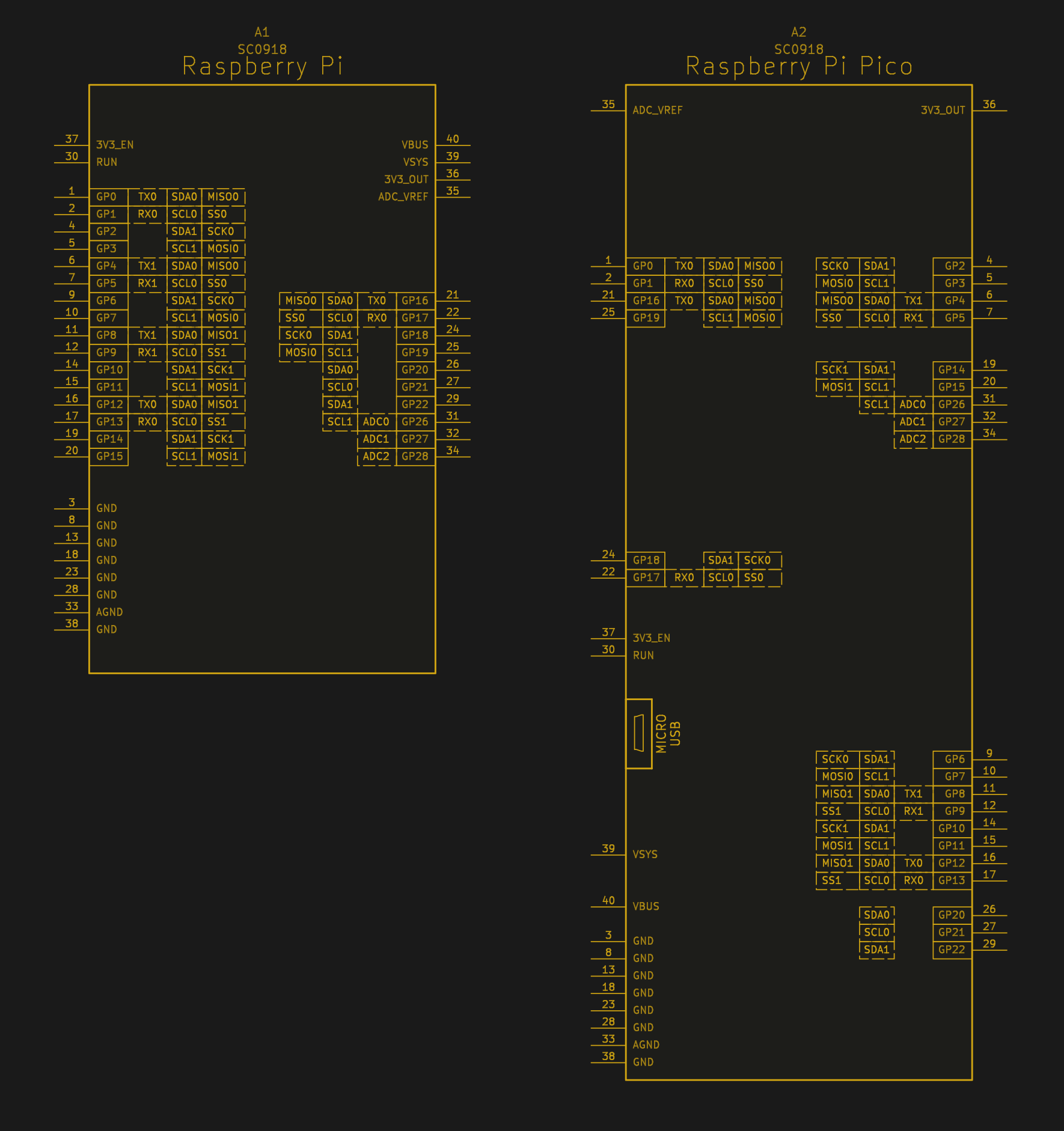
But probably the most helpful tweak is to simply rearrange the location of pins on the symbol and its size to better match your circuit. Consider the schematic symbol of a Raspberry Pi Pico module, which is arranged in a familiar pattern by GPIO number. Following that is the same Pico module after being tweaked to fit into the redrawn Vectorscope schematics.
Wrapup
There were a few issues between the original schematics and the PCB layout, but those have been sorted out. Some of the part footprints on the PCB are not footprints after all. Instead, they appear as a bunch of independent pads. And some parts have a discrepancy between the PCB pattern and the parts purchased from the BOM.
Just a few of the nets on the original schematic have names, and the rest are just blank. In the schematics, I tried to pick reasonable net names for the nets. I think this will be helpful when I eventually make the connection between the schematics the PCB.
At this point, I’ve completed what I wanted to in the beginning — make a KiCad schematic for the Vectorscope project. The KiCad project is not 100% consistent, but I have dug into the few missing pieces and solving those issues is not going to be a huge effort. These issues are explained in the readme of the project’s GitHub repository.


Nicely written article
“visual net lists” – not sure exactly what the author means by that, but what I find incredibly irritating is schematics where netlabels are used in a similar way to ‘global variables’ in a programming language to connect things together.
For instance, there’s a GPIO_1 well up in the left hand corner, and a GPIO_1 somewhere halfway down the middle (not connected by schematic line or bus), and it’s up to the reader to find out how they connect, and if they perhaps connected in 3 places.
Yes of course, if you have a pdf then you can perform a search. But a schematic should not have to rely on a search.
The cause for this complaint is that Kicad does not highlight the elements of a net the mouse hovers over. It is just a not user-friendly and cumbersome EDA.
I made a quick mock up https://ibb.co/yBFGP2T. With paint. Because I can.
To me, that is much more readable. Functional blocks are clearly separated and their interface to the outside is visible in one view. In a better EDA software the net lines would be highlighted when hovered. So it is totally clear, where the interfaces start/end/go to.
In that schematic the dashed lines around some blocks are a substitute for the function block separation. Because, readability. Why clutter the space with lines that go from here to there and do not give much more information than busA here and busA there? And add additional frames?
And lastly, this isolated function blocks make reusing/verifying/etc less difficult than first to make a separation process to recognize the block structure. A casual looker without knowledge of the entire schematic can clearly see a functional part. They might have knowledge about that part without understanding the whole thing.
But all IMHO.
The same schematic is supposed to work printed on paper or exported into PDF etc. and viewed by people who don’t have/use EDA software for any reason, so while having net highlighting would be nice for the designer, they really shouldn’t be drawing a schematic that needs highlighting to make sense of.
One feature from “old” schematics that I miss in modern EDA-prepared ones are off-sheet references. We have global labels, of course, so we know a signal is going off sheet. But schematics used to also show little “bubbles” which had a page and zone number (could be more than one set) of the other end of the connection. Like ” 4 / B3 ” to indicate zone B3 on page 4. Surely these could be easily depicted on modern schematics, but I haven’t seen it ( maybe this exists in other packages that I’m not familiar with ). The other feature I miss, which seems like it would be trivial to implement, are the “bumps” when wires cross over and don’t connect. That makes it so much easier to distinguish between a real junction and a crossover. I’ve also seen schematics prepared with a rule that “there shall be no 4-way junctions ever”, so any crossovers are by definition just crossovers.
About printed sheets vs inside the EDA tool, I remember one of the first computer-generated schematic projects I worked on, we were using OrCad. We had discovered the hierarchy paradigm, and went to town using it — probably more than necessary. Back then, our company used an outside guy to do the PCB design. I remember in our first meeting he was terribly confused by these blocks and just couldn’t wrap his head around them. Finally, we saw a light bulb go off in his head … he said, “So, you’re saying, if I throw away these sheets (a couple of pages with only hierarchy blocks and no components) it’s all good?” We scratched our heads a few seconds, and realized he was right (we didn’t have any repeating hierarchical blocks, or his suggestion would not have worked). He just left those two pages on the table and took the rest and got to work.
KiCad can show Intersheet References for global labels. Just turn on Schematic Editor / File / Schematic Setup / General / Formatting / Inter-Sheet References, and you can also click on those references to go to that page of the schematic.
That other thing, those “hopovers” are a horrible thing that are very luckily not used in any EDA suite I know. We’re living in the 21 century now and 10th generation photocopying of schematics is a thing of a long gone past.
And about hierarchical schematics. It is a tool, and it’s a useful tool, but any tool can be abused to make something horrible. Just look at what the arduino folks did to C++.
What we have instead is people taking a screenshot of a schematic and sending it by email, where it gets auto-compressed by outlook etc. which has virtually the same effect.
Worse yet, a cellphone camera photo of a computer monitor showing a schematic that was sent by email as a screenshot and compressed. “Hey, can you tell me what this component/symbol/part is?”
yup that is a nice looking circuit, and that is roughly what mine look like too, with deliniated blocks.
I make more use of buses though. Because extra lines (wires/nets/connections), I consider extra noise, where the ‘signal’ is the connectivity. The ‘signal’ to ‘noise’ using a bus can be better when using multiple lines, and also a bus can be given different colours, so easier to identify at a glance all the blocks on a page which connect.
Off-topic: a bit confused about the ‘shutup’ signal coming out of XM1. Its line seems to end on the SCL net, but there is no connection dot. To prevent confusion it should end somewhere more definite.
Wires are not noise. They have a function, when using wires, you can actually see where signals are going to, and how many connections there are.
you didn’t quite get my point.
EXTRA wires create EXTRA noise.
Yes all connections must be connected by wire or bus. But creating a spaghetti of wires reduced readibility, where they could be improved by buses.
mime… my term “visual net list” is, as far as I know, not anything official. It’s just an informal phrase that my colleagues and I have used over the years to describe this practice of not physically connecting the nets (lines) on the schematics. The result is usually a bunch of small islands consisting of a chip and short wires with net names. This isn’t terrible for a small circuit, but if the circuit is so small, it shouldn’t be hard to actually draw the circuit conventionally.
hi Chris, then we are on the same page. Visual net lists are aweful.
A good schematic has the right balance between nets that are connected with visible lines and ones that are connected by labels. Old style schematics had ever line draw. Usually they had two big lines for power. This restricts the layout of your schematics. I think power and busses, such as I2C, can be done perfectly with labels to prevent a criss-cross of lines. This allows easier grouping of sub circuits in a sheet and splitting large schematics in multiple sheets. Do you really need to see the positive and negative power rail of all opamps going to the power supply?
“the scourge of many schematics these days — “visual net lists” that are neither good schematics nor useful net lists.”
Couldn’t agree more. Where did this evil practice come from ?
Uggg. THIS.
I can’t even begin to count up the number of schematics I’ve seen where it’s just a page full of instantiated parts with little stub nets coming off each pin, and you have to search the entire schematic to figure out where ‘signal_x’ goes.
Sometimes this is OK, like with obvious busses, but I see it everywhere, even in analog circuits.
Booo!
I’d like to point out that the ability of the tool to let you jump across the page or sheets with only the net name connecting things can be useful at times. But it’s something that should be used sparingly, in my opinion, and not the default way of hooking up your components.
It’s not an evil practice. Using labels instead of visible lines to connect nets gives you more freedom in how you layout your schematics.
If you overdo it it will be bad, sure. But, do you really need to see the positive and negative power rail of all opamps going to the power supply?
It’s nice to order the gates of an IC in the same order and orientation they appear on the actual footprint, so you’re already seeing hints of the potential board layout in the schematic.
KiCad has more and better tools for this job then mentioned in this article.
I see the project has gerber files created by altium (https://github.com/Hack-a-Day/Vectorscope/tree/main/hardware/vectorscope/Gerber) Gerber files can be back ported into a KiCad PCB quite easily, but the conversion is not perfect, as the idea of “footprints” does not exist in gerber files. A few years ago I made a tutorial for it on https://forum.kicad.info/t/reverse-engineering-kicad-project-from-gerber-files/30903 Converting the other PCB copper to graphical lines for import in KiCad is not a very good thing to do. In the tutorial above I have also written how to replace the pads from the reverse gerber files with real KiCad footprints. (Which is an issue mentioned on the gitlab repository for this project).
And for the schematic. In KiCad you can add images to both the Schematic and PCB Editors with Place / Add Image and this is a nice tool for reverse-engineering Images can be scaled and you can put schematic symbols or footprints / tracks on top of it during reverse engineering. You can also rotate it if you want to change a “top to bottom” design into a “left to right” design.
On Gitlab you mention: “Schematics created, first pass error checking complete. It has not been meticulously compared with the original schematics.” There is no need to do so. If both the PCB and schematic have been (partially) reverse engineered, then just port the netlist from the schematic to the PCB and run DRC. It will tell you any missing or faulty connections if the two do not match.
I definitely was too quick with my previous post. I cloned the repository and just opened “Vectorscope/hardware/vectorscope/vectorscope.CSPcbDoc” directly in the KiCad PCB editor. :)
KiCad has direct import of eagle projects, and altium schematic and PCB files (altium projects is coming I think in V8, expected end of February) I did not know it can also directly import the circuitstudio PCB, but I just tried and it “works”.
For going forward, I don’t know whether it’s best to continue from the old conversion, or start anew from the direct PCB import. I have not looked at possible differences close enough.
All noted. I will check out your how-to guide in the link you posted, Paul. The PCB was not generated from Gerbers, although I can’t elaborate in detail about how it was made. Thomas converted the Altium project into a PCBNEW file, which did indeed retain the footprints as entities (for most of them). Some net names carried over, but not all.
About my “not meticulous” comparison, my worry there is that the original schematics have some small errors / omissions. I think we’ve identified all of those. I have made a branch and been doing a little more work on it, like running DRC. I have been on the cusp of “fixing” the PCB itself, replacing those items that came across the conversion with real footprints. But I haven’t jumped off that cliff, both for time reasons, and I’ve been slightly hesitant to branch the PCB. As it is now, if Voya came back with a modified design (and Thomas did his conversion again for me), it would be trivial for me to update my KiCad project. But after I change those parts, it seems that such an update is going to be a bit more cumbersome (maybe not, I haven’t completely thought that through).
I noticed there are at least 15 forks on gitlab. I thought git was meant as a tool to collaborate with other people. Maybe it’s worth to set up some communication on who does what. Maybe you can delegate the PCB design to someone else, in exchange for putting some extra effort into writing a new application. (Or the other way around).
No picture of what this thing is supposed to be or do? Weak.
The first line of the article tells you what it is and what it’s for. It’s an electronic badge for the Hackaday supercon. The badge is called the “Vectorscope.”
Nice work and writeup, [Chris Lott]. It’s always good to see some clever new tricks for Kicad! How close are we to a production run of these reverse-engineered badges?