Sometimes, a little puny matchbox-sized electronic speed controller (ESC) won’t do the job. If you find yourself looking for something heftier, say, in the range of hundreds of amps, you might look towards a design like the MP2 ESC. [owhite] has built an example of the design that can deliver some serious power.
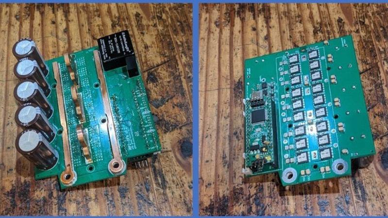
[owhite’s] build has some serious specs: it’s rated to offer up to 300 amps at up to 150 volts, though thus far, it’s only been tested at up to 100 V. Like the original MP2, which hails from the Endless Sphere forums, it’s designed to be compatible with VESC code using the STM32F405 microcontroller. It’s intended for driving high-powered traction motors in applications like e-bikes and electric scooters, as you might have guessed by its potential output power being well into the tens of kilowatts range.
If you’re eager to build your own, you can do so, with the design files on GitHub. Just note that you’ll need some hefty parts to handle the juice, including beefy MOSFETS and juicy capacitors rated at 160 V.
Open source motor controllers abound of late, and we’ve featured a few in recent times. Just remember that astute design and using parts within their means is the key to avoiding letting the smoke out!


I took a look at the schematic. No TO-220 packages, no heat sinks.
The power MOS-Fets are about $5 apiece on DigiKey, and you need 6 per phase (x3 = 18).
You will need bus-bars mounted/soldered to the board to handle the current – way more current than any trace could reasonably carry.
Lots of useful comments in the schematic. Looks like a very well laid out project.
MP2-DFN (the repo name) actually a DFN package variant of the MP2-ESC project which is here: https://github.com/badgineer/MP2-ESC
I’m not sure why they wanted DFN instead of TO-220 but that’s the big difference.
these probably support that current xD
https://hackaday.com/2016/12/16/massive-20-oz-copper-pcb-enables-electric-racing/
I would never operate this without some sort of busbar — I used 3.2mm copper that was cut at sendcutsend, then soldered on the underside of the board. They’re visible from the pic.
Go with 2oz or 3oz on 8 or 10 layers with 1″ wide traces and it’ll do 300A just fine. There are shipping industrial products that do just that, and with 480V in a 50C ambient too.
Clarification – no individual heat sink hardware bolted to transistor bodies.
An aluminum block is held against the transistors with a thermal pad, but without thermal grease.
Fan is still needed for cooling.
https://imgur.com/VpctpBx
It looks like a Work in Progress.
Buss bars are shown in the title picture of the Hackaday article, and there are DXF drawings for the bus bars. There is also a graph of 3 mosfet temperatures (without heatsink, with heatsink, and “heatsink + fan”. There are also some references to 3D models, but none are shown in KiCad’s 3D viewer
The git clone was a bit big, 280MB and 268MB is in the file “.git/objects/pack” I am not goo good with git myself, but with: “git whatchanged” it shows there are probably more then 300 copies of zipped up versions of the automated backups that KiCad makes in there. Putting that directory in the “gitignore” file would help a lot. I also see over 10 sets of gerber files without notes of why they were added. I normally only save sets of gerber files that are used for actual production of PCB’s. gerbers made for PCB review, are just intermediaries and not worth saving (in my opinion).
I do not understand the cutouts in the GND plane around the “pill” module. On some layers they attempt to isolate, while on others the GND plane is continuous. I am guessing that using no cutout at all is probably better. I also do not like the use of such a “pill” module for a project like this. Those “pill”s are fine for experimenting on breadboards and other things, but they are usually just dual layer PCB’s without a proper GND plane of themself. The original “Maple Mini” apparently had 4 layers too, but those have been unavailable for a long time.
I am curious what others think about this. Would you pay EUR1 extra for a “pill” on a 4-layer PCB with a proper GND plane? (and maybe some more GND pins too…)
But overall, I think I like the original MP2-ESC project better. It has a more compact PCB. uses TO220 and it has more room reserved for the BUS bars. But with currents this high, TO220 becomes a bit troublesome. It’s pins may start to melt. I also do not have enough experience to have a real opinion about this.
One thing I would do differently is to put the KiCad schematic in a hierarchical design. Put all the drive circuitry of a half bridge (including feedback amplification) on a single sheet, and include three instances of this sheet.
It really is not a work in progress. It fully works, and everything is there for you to build one yourself. This, and the original MP2 have propelled 10s of bikes and scooters around with ~10kW. Total builds I am aware of now are in the 20s. Maybe more I am not aware of.
The slit in the ground plane is very intentional and essential. If you consider what happens when you pass 300A through copper planes, say a total of 4oz between the layers, then you have about 0.125mohm/square. The link above the pill has about 4-5 squares, to you are looking at some 0.5mohm. 300A… that’s 150mV. Do you want that across your logic stage? with a ~+/-450A reading at 3.3V that is like 40A of noise/error. With the split… No error because the signals are routed as differential pairs outside the split off area. So it is plane; it is vastly better by trivial math.
Why pill? Well, pills work for one, they have the appropriate IO to avoid messing with USB, crystals, SWD… you can know with absolute certainty your design will boot. I have run an MP2 with several pills. The noise even at 100+A is small, the lack of ground plane is clearly not having too bad an effect. The reason for choosing them was interchangeability. When the MP2 was conceived, there were several open source software options in play (5+ including the ST and Infineon libraries easily useable with this), and the ability to swap in different pills with the appropriate MCU means it is possible to get actual comparisons.
Your point on the git ignore is fair. Your point on making it heirarchical… To what gain? Sure you could but… Why? It does not make it easier to read or adapt, and to propose doing it after the fact to make… making the design easier ?!?!
David Aka mxlemming on ES
You are mostly right. You also have spend a considerable time on this PCB while I had a brief look at it. One of the things I missed is that the in2.Cu layer under the pill is 3V3 zone instead of GND, and that explains the slot in that zone on the left side.
But still, removing the slot on the top side of the pill would reduce the squares from 5 to less then 2, but that is not fair because of the current concentration where it enters the PCB, and the addition of the bus bar trows off the calculation. A lot of the current will also be between the big electrolytics and the Fets. Adding the isolation slot is an easy way to avoid problems, and it turns the local GND for the pill into a sort of star GND.
For such a high current PCB, it also matters where and how the current enters the PCB. When the power cables are connected near the center of the PCB, this halves the average length the current travels over the PCB, and it also halves the current though the PCB tracks because half goes to the left, and the other half to the right, so that is a 4x reduction of voltage drop over the PCB. But with the bus bars it is apparently already sufficient and putting the power cables on the side eases cable management. Would moving the power entry to the center of the PCB be an issue in the intended application?
Another consideration is the GND pin of the opamps. I see 100k pullups on the non inverting inputs to prevent negative input voltages due to a lift of the opamp’s GND potential by the PCB current. Servo 57B (and C) use these pullups on both the inverting and non inverting inputs. This reduces the output offset voltage, but I guess it is compensated for in software.
About the pill… It’s good enough apparently :) and I agree that the ability to swap them also has an advantage.
The Hierarchical design… It does not make much sense to change it afterward but it does make sense if you do it early in the design. It ensures that all three driver circuits are the same, because you only draw one. Often incremental changes are made during the design. Small things around the fet drivers, swapping the fet’s themselves, other tweaks. and you have to do this 3x when the end stages are drawn 3 times. And ensuring the driver circuits stay the same during the design is a bit tedious. Using hierarchical sheets also enables use of the “Replicate Layout” plugin. It takes some time to get used to using this plugin, but it does speed up PCB design. With it, you lay out the footprints and tracks for one of the sub sheets, and the plugin replicates the footprint placement and track layout for the other identical sheet instances. And it can be run repeatedly, so it also helps with changes made during the design.
Part is also a personal preference. I have a relatively big (107cm) 4k monitor, and I still cant comfortably fit both the schematic and PCB editors on it with such a big schematic.
But overall, nice project and (at least) adequate PCB design. It’s easy to forget how the combination of Internet and and Open Source software helps with collaboration on projects like this.
This design looks like it could be serious competition with the 400 horsepower motor VFDs I work with that are massively large, heavy, and the price of a new luxury car…
You’re off by a factor of 10.
If you are interested in serious motor drivers, then have a look at Axiom:
https://hackaday.com/2019/11/04/axiom-a-100kw-motor-controller-fo-making-big-motors-move/
Sure if you’ve got a spare lifetime to wait.
anyone heard anything on AXIOM in the last 4 years? I made several attempts at acquiring a controller from them but never got anywhere. Their Powerdesigns website has sat unchanged and uninteresting for years. I assumed there was some fatal flaw in either the design or the company itself.
Unfortunately, yes you are off by a factor of 10 or more depending whether these industrial drives are 400HP continuous or peak.
The unfortunate reality is that for very high power, you just have to go to high voltage and accept the associated dangers. It’s actually easier once you understand creepage and clearances and isolation to work with high voltage because the currents are so much lower, and the effect of ringing and parasitic inductance get far less severe, and the amount of copper required for current conduction scales with amps not volts, so there are no greater conductor requirements (except you need properly rated cables and connectors for safety…). 50V overshoot on a 100 or 150V FET can be terminal… 50V on a 650V IGBT or MOS is basically irrelevant, so the layout is greatly simplified. There are 600V modules widely available that make design easier, and most gate drivers are optimised for 600V+ operation; we just choose to use them in the lower voltage range because they are cheap.
400kW will still be 400A at 1kV.
If you want to convert that to horse power, then first get some bales of hay.
“specs: up to 300 amps at up to 150 volts” looks like “china” specs.!
Actual data ,from datasheet, gives 95 Amps max @ 25C (junction temp).
IMHO it can work ,fine, on a e-bike with 36V and 1 kW motor.
I think you might be looking at the wrong data sheet. The one i have gives the chosen MOSFETs 117A continuous at 100C junction temp. And there’s 3 in parallel. And 3 phase phase currents are given as peak not RMS for various math reasons. And it’s time shared between high and low side MOSFETs… Also in fact the dcdc converter won’t even turn on at 36V because that’s below its 40V minimum rating so… Ummm… yeah…
Ya, These are 150V FETs: https://www.onsemi.com/pdf/datasheet/nvmtsc4d3n15mc-d.pdf
You don’t run FETs at the max voltage. 100V on 150V FETs is still pushing it.
Infineon sell a “HybridPACK” MOSFET array for EV’s ready to bolt to a water-cooled lump of aluminium that can do 100kW. Not sure what the list price is though!
It appeared in one of Munro Live’s teardowns of a Hyundai EV recently too.
https://www.infineon.com/cms/en/product/power/igbt/automotive-qualified-igbts/automotive-igbt-coolsic-mosfet-modules/hybridpack-drive/
Mouser says FS770R08A6P2BBPSA1 HybridPACK™ Drive Wave 750 V/770 A $483.56
Those look quite familiar to what is used in that “Axiom” project mentioned earlier.
Why do you keep chiping AXIOM AXIOM AXIOM? There is no AXIOM PROJECT. Theres a dead end page thats not responded to anyone inquiry in YEARS. Move on already.