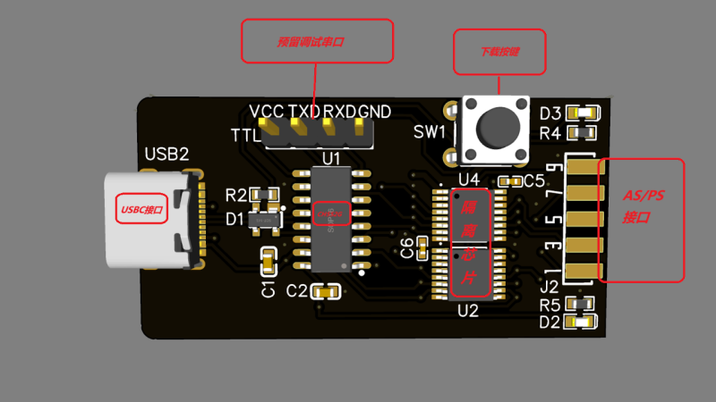
Here’s a CH552G-based USB Blaster project from [nickchen] in case you needed more CH552G in your life, which you absolutely do. It gives you the expected IDC-10 header ready for JTAG, AS, and PS modes. What’s cool, it fits into the plastic shell of a typical USB Blaster, too!
The PCB is flexible enough, and has all the features you’d expect – a fully-featured side-mounted IDC-10 header, two LEDs, a button for CH552 programming mode, and even a UART header inside the case. There’s an option to add level shifter buffers, too – but you don’t have to populate them if you don’t want to do that for whatever reason! The Hackaday.io page outlines all the features you are getting, though you might have to ask your browser to translate from Chinese.
Sadly, there’s no firmware or PCB sources – just schematics, .hex, BOM, and Gerber .zip, so you can’t fix firmware bugs, or add the missing USB-C pulldowns. Nevertheless, it’s a cool project and having the PCB for it is lovely, because you never know when you might want to poke at a FPGA on a short notice. Which is to say, it’s yet another CH552 PCB you ought to put in your PCB fab’s shopping cart! This is not the only CH552G-based programming dongle that we’ve covered – here’s a recent Arduino programmer that does debugWire, and here’s like a dozen more different CH552G boards, programmers and otherwise.


I’ve been using CH55x microcontrollers for a while now and used to put a program button on the PCB like in this project, but realized that the button didn’t have to be on the board so I built a tool to simplify programming: hackaday.io/project/192461-ch55x-one-click-program-mode
Hope someone will find this useful :)
It is quite easy to re-create a PCB file from a set of Gerbers in KiCad. I made a little tutorial for this a few years ago:
https://forum.kicad.info/t/reverse-engineering-kicad-project-from-gerber-files/30903
For a simple PCB like this it would probably take between 10 minutes and half an hour, after you have done it a few times and are familiar with how to do it.
But maybe this hackaday article motivates the creator to release more info about this project. The firmware is the most time consuming part.
Looks like a decent guide – was wondering about the practicability of reverse engineering gerbers; cheers.
What is an USB blaster? Like, IR blaster but then for USB?
The “Altera Byte Blaster” was a very simple dongle (74xx244 buffer on LPT) to program Altera logical devices. When the LPT got out of fashion this was changed to the USB Blaster.
A quick search:
https://duckduckgo.com/?q=ch552+usb+blaster&ia=web
Finds repositories appearing to contain SDCC source code:
https://github.com/VladimirDuan/CH55x-USB-Blaster
But overall, I’m not interested in 8051 stuff, which should have been obsolete and forgotten (or be an either cherished or cursed memory) for 15+ years.
>CHEAPEST USB BLASTER EVER
is it? FX2lp boards are $5 and work as USB Blaster. Recently covered “tiny FX2 boards” are $0.99 https://hackaday.com/2024/04/15/logic-analyzers-decoding-and-monitoring/
“Altera USB Blaster” costs around EUR3 from Ali, including the box, cables and shipping.
But overall, prices for such things are so low they are irrelevant. It’s much more important that you get a product that still functions properly.
Back when the “Blue Pills” were EUR3.5 they were very nice development boards, and now that prices have dropped below EUR2. You can get any chip on it from at least 5 different manufacturers, with the type number black topped and replaced with “STM”. Each variant has it’s own peculiarities and incompatibilities, and overall the product got completely destroyed by reducing the price another Euro. I’ve given negative feedback a few times, simply because they do not ship what I’ve ordered (an STM part), but a bunch of years it got so bad that I just don’t buy these boards anymore. Later I’ve bought a few “Black Pill” boards from WeAct Studio with a more modern STM32F411 and also some with STM32F431. I think / hope they are genuie STM32 parts (Price is high enough) but I have not used them yet and am not absolutely sure.