As great as silicon is for semiconductor applications, it has one weakness in that using it for lasers isn’t very practical. Never say never though, as it turns out that you can now grow lasers directly on the silicon material. The most optimal material for solid-state lasers in photonics is gallium-arsenide (GaAs), but due to the misalignment of the crystal lattice between the compound (group III-V) semiconductor and silicon (IV) generally separate dies would be produced and (very carefully) aligned or grafted onto the silicon die.
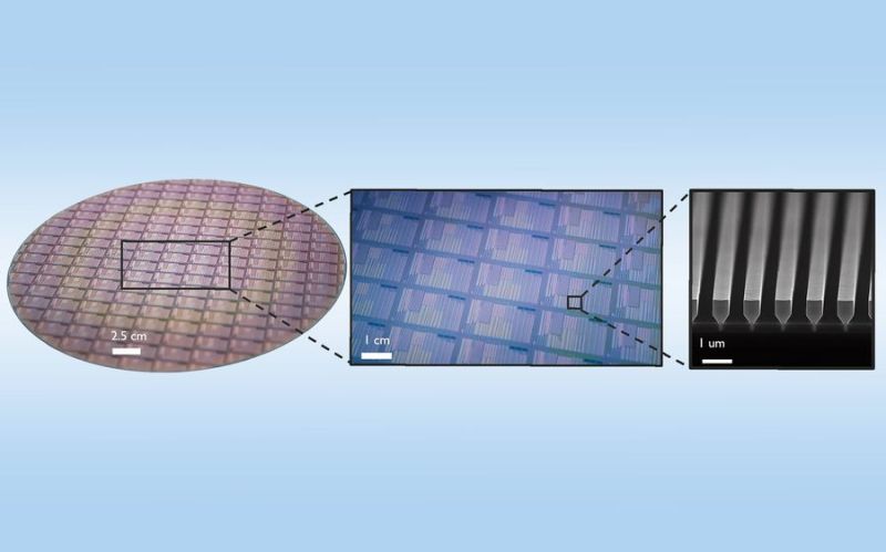
Naturally, it’s far easier and cheaper if a GaAs laser can be grown directly on the silicon die, which is what researchers from IMEC now have done (preprint). Using standard processes and materials, GaAs lasers were grown on industry-standard 300 mm silicon wafers. The trick was to accept the lattice mismatch and instead focus on confining the resulting flaws through a layer of silicon dioxide on top of the wafer. In this layer trenches are created (see top image), which means that when the GaAs is deposited it only contacts the Si inside these grooves, thus limiting the effect of the mismatch and confining it to within these trenches.
There are still a few issues to resolve before this technique can be prepared for mass-production, of course. The produced lasers work at 1,020 nm, which is a shorter wavelength than typically used, and there are still some durability issues due to the manufacturing process that have to be addressed.


How can you even do reaseach on semiconductor manufacturing those times? All of the equipment is at fabs which are guarded by heavily-armed private security. They’re not going to let some university professor derp around tinkering with their $5b machine when there are 3 years of NVIDIA, AMD or Samsung chips on backorder.
Also, it’s not like it’s 1950s anymore and you just add a bit of germanium or boron to a hot pot with molten silicon and build a working IC at university.
According to the article, this was done by IMEC, a world-leading semiconductor research company, presumably in their own state of the art fabs. They have 12,000 m2 of cleanroom. It’s not some “university professor derp”. All of which you could have found out if you googled them.
NOTE TO ED: I’d not heard of IMEC; maybe link to their Wikipedia page?
@Dan said: “According to the article, this was done by IMEC, a world-leading semiconductor research company, presumably in their own state of the art fabs. They have 12,000 m2 of cleanroom. It’s not some “university professor derp”. All of which you could have found out if you googled them. NOTE TO ED: I’d not heard of IMEC; maybe link to their Wikipedia page?”
Good point Dan. I am not the author nor editor of Rock Erickson’s post or this thread, but I can easily post the link to the Wikipedia entry on IMEC for you:
Interuniversity Microelectronics Centre (IMEC) is an international research & development organization, active in the fields of nanoelectronics and digital technologies with headquarters in Belgium.[1] Luc Van den hove has served as president and CEO since 2009. Imec has more than 5,500 employees and researchers for advanced semiconductor R&D activities, also including system scaling, silicon photonics, artificial intelligence, beyond 5G communications and sensing technologies. In 2022, Imec’s revenue (P&L) totaled 846 million euro…
[1] IMEC
https://en.wikipedia.org/wiki/IMEC
Dan, besides IMEC in Belgium, there is CES Leti in France, AMF in Singapore and AIM Photonics in NY ( part of NY CREATES). All are world class fab facilities that support semiconductor R&D with multi project wafers.
No, it’s not the 1950’s any more, and universities are not stuck using 1950’s equipment! Most of the basic research is still done on the small scale using modern equipment and a sea of cheap PhD student labour.
Then there are commercial entities like IMEC that bridge the gap between universities and industry. I was talking to a colleague at work just a few days ago who interned there as part of his PhD. Sounded incredible even though he was unable to actually go into any detail (half NDA, half because they wouldn’t even tell him very much!)
One factor that helps is that research processes don’t have to be commercially viable. Getting 200 billion transistors all working on 90% of chips manufactured is much harder than getting a research chip of 1 laser diode per chip working on e.g. 10% of chips.
Imec and ASML have joint ventures and labs, so imec has direct access to the newest EUV machines.
https://www.asml.com/en/news/press-releases/2023/imec-and-asml-sign-mou
https://www.asml.com/en/news/press-releases/2024/asml-imec-opening-high-na-euv-lithography-lab
Rock Erickson makes an excellent point. The people who would like to create chips, need “maker” labs. A “maker” lab might grow diamond (semi-conductor) circuits that might become the norm. All those PHDs need startup funding for such labs. The Chinese seem to be trying or succeeding at leapfrogging ASML methods. Maybe the young PHDs can too.
Is the GaAs single-crystalline, or polycrystalline?
Have they tried a checkerboard pattern, instead of ridges?
Shouldn’t it be: “a LONGER wavelength than typically used”? It depends on the application, but most applications still use blue/red laser light, “typically” around 450/660nm.