Let’s say you had a SNES with a busted CPU. What would you do? Your SNES would be through! That is, unless, you had a replacement based on an FPGA. [leonllr] has been developing just such a thing.
The project was spawned out of necessity. [leonllr] had purchased a SNES which was struck down with a dead CPU—in particular, a defective S-CPU revision A. A search for replacements only found expensive examples, and ones that were most likely stripped from working machines. A better solution was necessary.
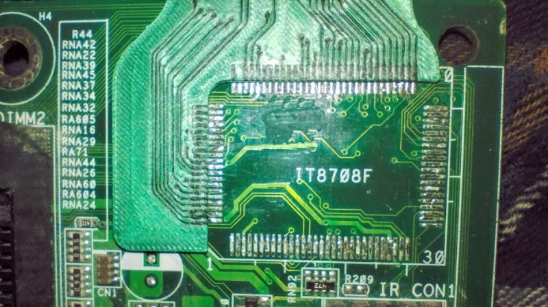
Hence, a project to build a replacement version of the chip using the ICE40HX8K FPGA. Available for less than $20 USD, it’s affordable, available, and has enough logic cells to do the job. It’s not just a theoretical or paper build, either. [leonllr] has developed a practical installation method to hook the ICE40HX8K up to real hardware, which uses two flex PCBs to go from the FPGA mainboard to the SNES motherboard itself. As for the IP on the FPGA, the core of the CPU itself sprung from the SNESTANG project, which previously recreated the Super Nintendo on Sipeed Tang FPGA boards. As it stands, boards are routed, and production is the next step.
It’s nice to see classic hardware resurrected by any means necessary. Even if you can’t get a whole bare metal SNES, you might be able to use half of one with a little help from an FPGA. We’ve seen similar work on other platforms, too. Meanwhile, if you’re working to recreate Nintendo 64 graphics chips in your own basement, or something equally weird, don’t hesitate to let us know!


Was the Dr. Seuss rhyming on purpose ?! :D
Consider what day it is.
Flex PCBs have ridiculous tolerances on vias/etc. since they’re laser drilled, so you can slot the pads and lay it on top. In this case if you can find a connector with enough pins for the connection, you could just drop the connector in the center and it’d just overlay the CPU footprint entirely.
It’d be a bit of a dense connector but not that bad. Maybe fit two if needed.
Even if you come in from the side like that, slotting them (like castellations) is a nice solid join. Since flexes can be cut with scissors you don’t have to have them cut at the manufacturer, you can just cut them to size afterwards (so they’re just normal pads and then you cut across them).
Pay me 20 mBTC or I’m going to climb my local GSM tower, smoke weed and wet my pants.
I prefer pickle Rick over 7 year old Rick
Also I will say I have my doubts this’ll work easily: even though the overall clock seems slow, the bus clock’s ~20 MHz and adding probably several nanoseconds round-trip for the level converters + in/out of the FPGA could kill the timing in some situations. Big difference between trying to logically emulate a full digital system and trying to emulate a portion of it.
If I were the author I’d really consider going with a larger FPGA first.
Thankfully on the S-CPU the bus access are clocked at about 3.5[MHz]
Um, no? Why do people say this? It’s like, everywhere, and it’s not in any way true. There is no 3.58 MHz clock on the system.
The SNES CPU is clocked at around 21.477 MHz. That’s what it runs at. Period. Always. The end. Its instruction/bus access timing is either 6, 8, or 12 clocks, so the CPU’s instructions/sec and IO/sec are less than 21.477 MHz. But the bus is 21.477 MHz.
(This is why insane emulators like bsnes run so much slower, because they’re literally bus-cycle accurate, which requires a ton more processing).
The internal logic to the FPGA is easy, because you’ve always got buckets of time (from the CPU’s perspective) to do everything you need. But the I/O is always the issue, and I/O on an FPGA is not as fast as you think it might be, because you need to route.
Especially on a very dense design if you don’t have I/Os ready at the output FFs to be clocked out, their output timing is going to vary wildly because they have to route from random locations, and that route time can Be Large – I’ve seen upwards of 10 ns, which when you combine it with the in/out through the level translators is going to push to 15-20 ns, which is now a large fraction of that bus clock.
Normally I’d say “but it’d probably be fine” but when you’re interacting with real hardware, I don’t know. It’s just trickier. Things that make an emulator glitch crash the system.
(By ridiculous I assume you’re saying the tolerance is good)
Thanks for your advices, what worries me a bit tho is my own precsision when designing the pads, I basically took the kicad footprint, cut it in half, and carefully moved the sides to put then in/outward of the original footprint,
I haven’t really realized this fact but do you think leaving the pads longer and more overlapping would still allow for easy solder ?
Yes, the flex PCBs from JLCPCB for instance have min drills of 6 mils (0.15 mm). I’m pretty sure the SNES CPU is just a 14mm x 20mm TQFP-100, so you should be able to just look up the package footprint from something else. Hilariously if it is a 14 x 20 TQFP-100, I’ve literally done this with that exact same package (obviously different chip). 0.4 mm width, 1.45 mm length, slot of length 1 and drill 0.15 mm. Round the corners for niceness.
The best thing for pad design isn’t overlapping – you want to give the solder as much surface area to grab on as possible between the two. That’s why I’m saying you put slots in the pads (dunno how to do it in KiCad but it should be easy).
The biggest benefit to the slot is that it’s plated: no matter what, if you’ve got pads that just “butt up” against the edge, you’re trying to make solder flow from the pad across a gap that is not metal. The bond is just solder.
You can make it work: I have! But oh dear God it’s fussy. It’s even worse on the SNES because this was back before the days of even remotely decent solder mask and so you can lift those pads So Freaking Easily.
If you’ve got a slot that’s plated, though, there’s metal to metal contact all the way from the pad on the SNES to the pad on the top. The solder will happily flow and form a nice fillet bonding the two.
“Let’s say you had a SNES with a busted CPU. What would you do? ”
– keep it for spare parts
– try to adapt a clone CPU from a defective clone console? Or try to get it from China?
I’ve tried to source clones for the S-CPU, but I didn’t find any.
Also, It’s very likely that the snes clones uses only 1 chip for cost effectiveness, rendering them unusable for spare part sourcing.
AI? Feels like a generic comment unrelated to the article.
Now that you mention it.. Yes, it reads a bit too sterile.
The correct use of commas is unusual for English people, too.
As a non-English native speaker I didn’t immediately realize this, though.
Please, if you read anything from me, like you are doing right now, keep in mind that I am not a native English speaker, that I have gained most of my English writing skills by reading databooks, political dissertations, Jack Vance, H.P. Lovecraft, J.K Rowling, and J.R.R. Tolkien, and that I believe that the proper use of commas, like I am displaying here, is important to the extreme. :D
No AI was subjugated into writing this.
Since you invited pedantry, many of those commas should have been semicolons because you nested two lists.
Yeah, this looks so generic, I would even think this would be a comment from an article on the S-CPU itself