We often think that if a piece of software had the level of documentation you usually see for hardware, you wouldn’t think much of it. Sure, there are exceptions. Some hardware is beautifully documented, and poorly documented software is everywhere. [Graham Sutherland’s] been reviewing schematics and put together some notes on what makes a clean schematic.
Like coding standards, some of these are a bit subjective, but we thought it was all good advice. Of course, we’ve also violated some of them when we are in a hurry to get to a simulation.
Most of the rules are common sense: use enough space, add labels, and avoid using quirky angles. [Flannery O’Connor] once said, “You can do anything you can get away with, but nobody has ever gotten away with much.” She was talking about writing, but the same could be said about schematics.
[Graham] says as much, pointing out that these are more guidelines. He even points out places where you might deliberately break the rules. For example, in general, wires should always go horizontally or vertically. However, if you are crossing two parallel wires, you probably should take advantage of the diagonals.
So what are your schematic rules? Software has standards like MISRA, CERT, and various NASA standards. Oddly enough, one of our favorite quick schematic editors is truly terrible but obeys most of these rules. But you can surely do better than that.


I like to make an “edit history” layer to document the changes I make, which I guess you could skip with careful use of git or equivalent…
most of the times you print the schematic to have it on the bench… it would be a PITA to go back to the computer, type git commands (or even use a GUI…) to see if your afterthought on that R22/C1/whatever value made your circuit a cumbersome doorstop. :)
Could you skip that with Git? I mean.. technically, sure the information is there. What are you going to do, grab old commits display in a second window and eyeball compare? Or read the xml of your favorite EDA tool’s schematic format in the diffs? That does not sound very efficient.
In work we use Altium which has subversion built in. or a cloud git based version control. It was a hard deal to sell version control on none software? we also collect issues and change in a document for any future re-spins.
Overall, good advise, clearly drawn schematics make projects much easier to read by others, and also when you see your own schematic a few years after you’ve drawn it. I do have a bunch of additional remarks though:
Be consistent.
In some of his examples he added the greek Ohm to resistors and F to capacitors, in other examples he did not. I prefer to use RKM code https://en.wikipedia.org/wiki/RKM_code It’s less typing (especially for the weird “Ohm” symbol) and uses up less paper space while still being very clear and unambiguous.
But with one small deviation. Using a capital K (Kelvin?) instead of the lower case k for the kilo range is clearly a fault in the “standard” Graham has also used both capital K and lower case k throughout his examples.
In addition to his rule 7). Symbols are logical, footprints are physical. Use standardized symbols. Sometimes I see opamps and FET’s drawn as rectangles. Yuck! always use the standardized symbols when they are available. Especially with the EasyEDA he uses this is somewhat common.
Put the value field of resistors inside the resistor. KiCad has both an “R” and an “R_Small”, but with the bigger resistor, the value fits inside the resistor, which makes the overall space used smaller with the bigger resistor. (It’s the default, but you have to turn off the “auto-placement” for the fields.
I agree with his “Split bigger schematics up into labelled blocks”, but the example he gave is very bad. He uses the “very many unconnected tiles” approach here, which is unfortunately becoming more common. Just try to figure out how the power is distributed from the input (USB-C?) to the uC (I could not find it). And how does that loose block with the USB jumper fit in the overall scheme? Every little block is connected with labels only, and this makes it very easy to miss a few connections. You have to use search functions to make sure you did not loose anything. Drawing all the rectangles is also a waste of time. By the time the schematic is finished, most of these rectangles have probably been redrawn more then 5 times.
Also, labeling a 3V3 regulator with the test “3V3 Regulator” is not useful. It’s much better to create a single block (or even a sheet) for the whole power section. That would include the “USB-C Power” block in the lower left corner, and the the connector. (Uhm, I think that block is the connector, but I’m not sure).
Making a bigger block with all the sensors combined also make more sense. Now you have to go hunting (zooming scrolling) to see how many sensors there are. Maybe there are more sensors on other sheets (the uC also seems to be missing…).
Just try to figure out how I2C is connected to all things. There is a “GPIO Net Ties” block, an “I2C Net Ties” block, an “I2C Logic Level Translation, and that is before any wire is connected to any IC. Having all these blocks (including the I2C sensors) connected with a few wires is very much easier to read. This schematic with all the little squares is a good example of an over use of labels, and this is a quite bad (but all too common) practice
Make the text in the titles bigger, so you can also read them when zoomed out. They really should be readable in the zoomed out picture he has shown on his website.
And maybe, just maybe, his block with “Plusivo ESP8266 Connector” is his microcontroller. Searching the internet reveals that it is indeed probably true.
Yep, splitting schematics into 3-component chunks with net labels seems to be the norm just now, it’s murderous to review and debug with. Keep whole systems together even if it’s a bit more messy. I’d rather have the whole power section on one page than break it down to 12v, 5v, AC subsections. Sometimes it’s just easier to see the lines joining 4 components than it is to mentally maintain that link.
I hate those thin multi-sheet schematics with a passion. I strongly prefer going up in sheet size over stacking multiple sheets vertically, hierarchical or not. And large format printers are a thing. One PCB, one schematic, darn it!
But the reality is that most designs these days are not only so complex that they don’t fit on a single sheet no matter how gargantuan, but most designs are being worked on by multiple designers in parallel. And my disdain for multi-sheet schematics notwithstanding, what’s even messier than those, is the result of multiple engineers with multiple styles working on one big sheet.
Unfortunately you need to use a pen plotter or even worse, an inkjet printer for anything larger than A3.
Lol, I was the lead firmware engineer for a project that had 80-100 page schematics. That isn’t going to fit on a large page.
It may be “the norm” just now, but in 1985 I went to work for a company that made engineering workstation computers, and most of the schematic pages had one component on them. At best there might be four, like four 8-bit latches connected to the data bus. It was brutal, since I had to use these for troubleshooting failed boards.
Going back even further, in 1976 I worked on the AN/UPX-14, which was an “interrogator/responsor” for the identification of friend-or-foe in a RADAR system. In the schematics for this, often whole pages had nothing but wires on them, which detailed the interconnections. But it meant that to find where a signal that didn’t look right came from, you had to go to the page where you see the signal, trace it back to a connector, go to that page, trace it to another connector, repeat 3x, and eventually get to the module it came from. They spent a day in class teaching how to do this.
Really quick one but I may be back for more comments.
No 4 way junctions. If you need 4 lines connected. Offset one of them one grid.
Nothing wrong with 4-way junctions. The days that junction dots (dis) appear by photo copying a flattened tree carcass (RIP) a lot of times is not a problem anymore in these modern times.
But please don’t start adding inductor hop overs, especially when a wire crosses a whole group of wires this makes schematics confusing, and they add nothing to the readability of the schematic.
Well its also about readability isn’t it. I agree there are cases where 4 way junctions may be acceptable (the exception to the rule) or even desireable, but generally just don’t do it. Not because of copying reasons, but simply to avoid confusion.
BTW, i don’t know where the rule came from, but my assumption here is ‘is this line crossing?, should this line have been crossing? Kind of situations.
I agree with paulvdh. Offsetting them to avoid a 4-way just makes the drawing more cluttered. The hops are also unnecessary. I arrange things for the lowest practical number of elbows and line crosses.
These are good. Gnd symbols pointing up make me physically ill.
There are at least 3 types of ground symbols. I’ve never been happy with the arrowhead type because it looks too much like “this wire goes somewhere else, maybe off the page.” Another type might indicate “chassis ground”, consisting of a horizontal bar with 3 tilted slashes below it: OK, if you must. I prefer the 3 or 4 horizontal bars of descending length.
True. If I absolutely MUST have a four-way interconnect without offset (very rare but it happens), I do it like so. Let’s see if the code formatting backticks allow me to maintain the monospace formatting..:
‘ | ‘
‘ | ‘
‘ ___/| ____ ‘
‘ |/ ‘
‘ | ‘
‘ | ‘
#fail
That turned into a train wreck.
There must be a tag for code notation, but I don’t know it. Is there somewhere an overview with all the allowed tags and their usage?
Please draw the gates. For example, if you have a 74xx00 quad NAND gate, do not draw a rectangle with the A1, B1, Y1, A2, B2, Y2, etc. down the sides of the rectangle. At the appropriate places, draw out the individual NAND gates with the NAND schematic symbol (square on the input end, round on the output end, with the little circle at the output indicating the inversion). This will also reduce the connecting lines’ lengths since they don’t all have to come to one rectangle, and it will make things easier to follow. (This applies to ICs having multiple individual gates each. It would not apply to ICs where the whole thing works as a unit, like the 74xx138 3-to-8-line decoder, the ‘245 octal tri-state transceiver which is intended to be used on a bus and has a single direction pin and a single enable pin for all eight buffer bits, the ‘595 8-bit shift register which has a single pin for each of five input functions and serial out, applying to all 8 bits of the one shift register, etc.; but please do separate the two sections of a ‘139 dual 2-4-line decoder, a ’74 dual flip-flop, etc., even though each section will be drawn as a rectangle.)
Post or publish schematics with black lines against a white background. A few potentially helpful members of a forum I moderate have color blindness. One of them cannot see green lines against a yellow background, and has other color difficulties too; but people post their schematics in these troublesome colors. I have told Cadsoft/Autodesk about this problem and asked them repeatedly to change the default colors; but they apparently don’t care. If you post your diagrams in black and white, everyone can read them. I personally am not colorblind, but it still slows me down if some (or all) of the text is in a light gray font. The light gray pin numbers and labels on the ICs are awfully hard to read sometimes, so it would be good to darken them up. As I was writing this, someone posted a schematic with a black background and pin labels in dark blue. I could barely see there was something there, and I couldn’t read them without getting off my chair and getting up really close to the monitor.
A common request on the above-mentioned forum is to have others look over their “schematic.” I put “schematic” in quotes because so often what they present is not really a schematic so much as just a netlist written around boxes, with tags everywhere, and it is very difficult to follow, requiring us to search the whole thing, sometimes several pages, for a matching tag. Please do a real schematic. Also, try to minimize the number of pages. I do large pages; but to get them printed, you might have to go to Kinko’s or other office-supply store where they have printers that can handle paper that’s 24″, 36″, or 48″ wide. I spent 38 hours on a work project doing nothing but searching for matching tags on a large schematic someone had drawn in lots of pages with lots of tags. I was consulting and was getting paid $100 an hour; so that was a very expensive waste of time, writing a long list of X-Y coordinates of tags on the many pages.
Eons ago, EU tried to standardize logic gates to be all rectangles instead of the specialized shapes for logic type AND, OR, NOT, XOR etc and I know that never settled well with me so I assume it’s the same with other folks. I’ll be using the old symbols till I die.
TI tried to push a different “standard” in the 1980’s also which (I think fortunately) never fully caught on.
I like to use hierarchical blocks instead of little functional blocks scattered around a page. My designs rarely fit on a single page anyway, and I end up with a top layer that gives a nice block diagram like overview of the design.
Another use for hierarchical blocks is to clarify multi-purpose processor pins. The default symbol may well have a pin labelled RD1/ECCP3/P3A which is no real help to the poor technician who is trying to understand what the function actually is. Placing this on a sub-block and connecting it to a net labelled RTS makes it clear that it is a simple digital input handling an RS232 handshake line (taken from an actual schematic).
i dispise the “no wires, all labels” schematics. try to fint where a signal is going is a hell.
Exactly. I spend more time than I should rearranging the parts on my schematic so that wherever possible I can draw a net without having to use a label. Of course I mostly so label every net because it helps when doing the layout.
Yes exploded schematics suck. If it is a modular build them put a dotted box around each module, fully interconnected.
Dangit, I’ve been moving towards no wires all labels. It’s so much less confusing for me but you do have to put some thought into what the label says. I usually have a two-part naming convention of some sort so it’s obvious.
But it would be nice if there was a command in the software that would highlight all the connections like notepad++ highlights all instances of what you’re searching for.
or if some KiCad developer was bored he or she could spend some time creating a smart switcher that automatically converted the schematic between labels and traces or even just have a fancy blinking temporary trace to show the connection. But I know there’s no such thing as a bored KiCad developer.
The point being it could be fixed in software :-)
In most PCB CAD software, if you go to the layout tool and highlight a pin, it will show the whole net that is connected to it. Not that you should ever have to do this.
Incidentally, if you don’t put labels on your nets, the application makes up names for them, and these are generally useless. Always label, even if you have to make the label invisible.
True that, obviously the labels help but it is super important that 1) the label names are descriptive and make sense and 2) the circuit is broken into logical blocks so you at least have some idea where to look for the matching signal label. Having stuff all over the place is asking for trouble.
The same can be said for programming.
I find the biggest issue when reviewing PLC code, whether it is RLL, function block, or structured text, is sticking to a “standard”.
Whether that standard is already existing or your own, if feel you must. If you’re going to use it then commit to it.
The purse of a tag/object should be easily recognizable.
SYS1_Inlet_Valve_0
vs
SYS1INLETVALVE0
PLC code tends to be iterative as new systems, similar to previous are added over time.
I hate going in to see:
SYS1_Inlet_Valve_0
SYS2_Inlet_Valve_0
SYS3_Inlet_Valve_0
SYSD_V0_IN
SYSE_V0_IN
Naming conventions are just as important as comments and descriptions.
I find the human eye (brain) does rather well with pattern recognition. When I’m scrolling through code during a troubleshooting session I’m internally saying/hoping “one of things is not like the other”.
Consistent adherence to a standard makes this easier.
With regards to creating the SCADA/HMI/Mimic the rules for layout still apply.
Flow should be in the same method as P&ID (schematic) layout. Left to right, top to bottom.
Flow comes into the top/left and goes out bottom/right. Drains should be positioned like grounds.
If possible design the screen with the same view as looking out a window. Don’t reverse the two.
I’ve come across absolutely terrible code that I have no clue as to how it’s working at all.
I’ve also seen incredibly complex code that lacks any comment at all but strict adherence to naming conventions and standards made it very easy to troubleshoot and understand.
I would kindly ask that when folks publish their schematics as PDFs/BMPs, that they generate these in monochrome (or at least have a monochrome version in addition to the colour one). The dithering of yellow wires and beige backgrounds is hell to read from a laser printer output.
Another way to do the bus-flip from point 6 is:
https://prive.bitwizard.nl/bus_flip.png
I’m an EE, I think its pretty good advice on the whole. But with all these guidelines, a big mistake I see people make is to follow them blindly. The top priority is making your design readable and unambiguous. I see this mistake most often with mechanical drawings, where novices obsess over following the conventions exactly. Your design is meant to be read by a human! Just a put a damn note! And be done with it, or break a rule if you have to, as long as the result is clear. Imo his advice about additional annotations and notes showing WHY the values are what they are is critical. Years later you will have to make substitutions or modifications and you will not rememeber whether some random cap is a critical value or just whatever was convenient at the time. Add a lot of notes! I like to give every part a requirements property, that states the minimum specs. Voltage capacitance footprint tollerence, etc.
my struggle is text…i don’t draw schematics often enough to learn schematic software. and anyways, i don’t want to use something that doesn’t make coherent diffs when checked into git. most projects, i start a diary in a plain text file. i seem to have done just about every convention i could think of, at some point or another.
as an emergent thing, it seems like if i’m doing digital then it seems i tend towards netlists. very similar to the “3-component chunks with net labels” that everyone hates (myself included). but i don’t usually do it as a picture. a lot of times i have just sequentially listed all of the ICs in the circuit and for each pin i say what it connects to, whether it’s a pin of another IC or a power supply or what-have-you. if inter-IC connections dominate, then that produces a lot of redundancy.
if i’m doing analog design, i’m more likely to do ascii art, | and -. i try to avoid drawing components.
transistors are 3 lines labeled B E C. resistors are just Rn, capacitors Cn, etc. it gets unwieldy quickly, but luckily i’m not much of an analog designer anyways, so my circuits are simple.
i think i want a schematic description language, something like openscad but for drawing schematics. but i still haven’t thought of the root idioms for such a thing (the simplifications that make it convenient and intuitive to use without handicapping its expressiveness irreperably), and the few attempts i’ve run across haven’t floated my boat either. it seems to be a kind of unique problem domain in a lot of ways.
but even if i had such a language, wouldn’t i spend more time interacting with the schematic’s source code rather than the final view of it? the translator almost seems like it would be a waste, i want a circuit description language that can be read and written as easily. so it’s fully expressive and editable in-line with the rest of my diary.
I used https://mirrors.mit.edu/CTAN/graphics/circuit_macros/doc/Circuit_macros.pdf — you describe how the schematic looks like and the description compiles to a nice picture. It is not like doing an ASCII painting, though…
oh that’s interesting! thanks! not sure if i’ll use it but definitely reflects a struggle with a good set of simplifications
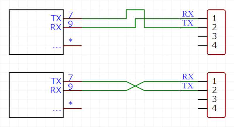
Whatever your intentions are, it should start with correct connections at all. In the example on top of the article, tx and rx are never ever connected to the same name. Maybe the names of “tx=transmitting and rx=receiving” was not clear enough?
heh if the left hand and right hand blocks are both ICs then yeah you’d usually want RX connected to TX? but if the left hand one is an IC and the right hand one is like a 4-pin header…
Sam’s Standard Notation has always been the way.
One thing I think a lot of schools are missing, when teaching students in electrical disciplines, is showing them what excellent schematics look like, i.e. examples from industry. Having a look at old schematics by companies like HP/Agilent, Tektronix, Fluke, Simpson, etc. in my sophomore year really opened my eyes to what was possible, and what should be expected of good engineers.
Also, ANSI Y32.2-1975 ’til I die.
As a software person I have only one thing to say to you – tabs or spaces?
Software people will fight to the death until the end of time over that one. It makes your differences on schematic standards seem trivial.
What we are doing is combing two Concepts into one diagram: WHAT we are doing (functional description) and HOW we are doing it (by connecting which wires, where? – the netlist) Because a Schematic generally has to perform these two simultaneous functions, I lean toward the functional description, as just a bunch of wires connected to nodes is… not especially helpful, alone.
I think Schematics can serve this function, and one more: Documentation for the tech / assembler. I do NOT understand why we don’t, universally, include PICTURES of the components we are using (along with full part numbers / URL to Mouser etc). Then when we are rummaging around a PCB, we have a visual AND a set of connected pins. For SMT caps, say, (since all 0204 part look the same) – give a little cut-out of the PCB surrounding area and highlight the particular component. The days when a silkscreen could reliably ID parts on a PCB are long gone, because the lettering is too small — and with parts squeezed in like sardines — there is no room.
I completely disagree that VHDL (or, as God uses, Verilog) is a ‘better’ description. For a HW person coming from a SW background, perhaps. But, a Block Diagram with signal flows captures operation better for me — especially in fully parallel FPGA code. Each block is a Verilog module, with identical I/Os etc. Straightforward, useful.
But don’t worry, soon AI will be generating weirdo circuits straight to PCBs that nobody understands that are the response to a Prompt: “Build me a 95% efficient switcher taking 5-25 Vin and producing 3V3 and 1V8 out in a 1 cm**3 space” — it can almost do exactly that today. (The observation I’m making is: We see very little of how AI is used in EE design – we need much more instruction on this subject.)
Schematics are very important. In large projects like powerplants, you will have schematics of the structures, the fluid systems, the electric power systems, the control systems, security systems, safety systems, HVAC (a fluid system), and maybe even other systems that are specific and/or esoteric. They are ALL important, and they cannot be reduced to one standard. You can layer several functions on to one another on paper, or on a computer CAD system, but it is bad to include everything in only one enormous drawing that cannot be separated out by function, or by system. You also want to make sure that they are useful, above all.
I was surprised to see that almost all of the rules proposed in the article I had incorporated into my own internal rules list. The only one new to me is using diagonals to show where two signals swap, which I hadn’t considered before, but think is a good idea.