Breadboards are great, but as the world moves more and more to having SMD as a standard, prototyping straight PCBs is becoming more common. If you’re mailing off to China for your PCBs, it’s shockingly quick for what it is, but a one-week turnaround is not “rapid prototyping”. [Stephen Hawes] has been on a quest on his YouTube channel for the ideal rapid-prototyping PCB solution, and he thinks he’s finally got it.
Now, if you’re only doing single-layer PCBs, this is a solved problem. You can mechanically mill, or laser cut, or chemically etch your way to PCB perfection, far faster than the Chinese fabs can get you a part. If you want a double-sided board, however, vias are both a pain in the keister to do yourself, and a rate-limiting step.
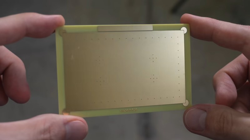
[Stephen Hawes] hit on the idea of buying a bulk set of PCBs from the usual vendors. The boards will be simple copper pours with vias in a grid with just a bit of etching. PCB Vendors are good at that, after all, and it’s not going to cost much more than raw copper. [Stephen] then uses the template of this “viagrid” board to lay out the circuit he’s prototyping, and it’s off to the races.
Or, off to the laser, rather. Unlike the fiber laser he showed us previously, [Stephen] is now recommending a diode-pumped solid state (DPSS) laser, as they can blast the copper off without burning FR4 substrate. Given that the vias are now part of the design, everything needs to line up perfectly, so his viagrid PCB design has a few features to lock it in using LightBurn’s “frame” feature. The DPSS laser barely shows up on the copper, but shines brilliantly off the fiberglass, and viagrid takes advantage of this fact. He’s also got a 3D printed jig to hold everything in alignment once it’s dialed in, even for running off many boards.
This laser is just as fast as the fiber laser, giving you PCBs in minutes. And while vias are apparently best left to the professionals, through-hole components can easily be accommodated, with the laser able to cut the FR4 on request. All of his lightburn and files for the varigrid PCB are available on GitHub. [Stephen] is also looking for collaborators to see if this technique can be used without the very-expensive Commarker laser, and to come up with a better name than viagrid.
As [Stephen] says in the video, if you combine this with a pick-and-place and a reflow oven, you can go from design to a working two-layer PCB in about 90 minutes, which is a very exciting prospect for engineering companies and maker-spaces alike. Words like “game-changing” get thrown around a lot, but this just might warrant it, at least for those who have a need for speed and can afford the tools.
What do you think? Is viagrid the rapid-prototyping revolution we’ve been waiting for, or is the headline of this article still subject to Betteridge’s Law?
Thanks to [Keith Olson] for the tip.


The beauty of this is now that he shared the idea literally anyone can make something using this. Also ripe for tweaks like a middle ground/power layer.
This is very cool. I however do not know how I feel about having to own a high power laser to make a PCB at home. Plus templates are just…I don’t know feel weird. But then again, I haven’t made PCBs at home in years.
Using this technique, you would be obviously locked into the stackup of the original templates, and the max number of vias present in the template. You can’t make anything too complex like HDI boards, or BGA parts which require precise soldermask (unless the laser can also burn away soldermask after you manually put it on?). Impedance controlled traces can be done since you know the stackup I guess, so low GHz ISM stuff is possible. Also no silkscreen, not a big deal
Maybe I’m getting older but its not as exciting to me, as it would have been 10 years ago. I would have been on cloud nine if I knew there was something that could let me do this…
I’m not keen on the idea of having to own a high power laser for this, there are much easier and cheaper ways to make good quality double sided PCBs at home for a fraction of the cost.
But it is cool and the ability to “drill” the board is nice, I wonder if the edges of the holes are carbonised enough to allow electroplating vias…
Well nothing about this method actually requires the laser, you could still etch or mill the two sides if you wished to as the real trick is the via grid that lets you have that 2nd layer of complexity more easily.
I don’t get the feeling that this is aimed at the home hobbiest, especially not at the prices for the laser. But for a business where time is literally money, being able to turn around prototypes in hours vs days can make this a compelling proposition. Very few are going to use this for very complex designs, but for quick confirmation that a part works as expected, or for debugging parts of a circuit, perhaps, I could see this being useful.
And I do also think that the concept is the powerful thing – companies with different requirements will refine it for their needs – extra layers, more vias, some standardised footprints and breakouts (potentially on multiple layers) for common components, etc. Come up with your own template for the FPGA or whatever ICs you commonly build around, leave space for the unique requirements around it, and order a bunch at the beginning of the project. Those arrive in a week, while you are getting some initial schematics sorted out, and from there, you can iterate every two hours.
This is why we have a small pcb milling machine at work. Vias and double sided cut, from schematic to board in usually two hours more or less, and it’s really been useful for development. We’ll go through five board designs in a couple days and when we have one that works, it goes out to the pcb fab houses for 100 copies.
Who doesn’t love the smell of vaporized copper and epoxy in the morning…
You don’t have to have a high power laser to make use of this idea – you could still use toner transfer and chemical etch. You could design your own via template, possibly even with an adjoining TH protoboard are (though that would be really fiddly for masking when etching, vinyl sheet or some spray-on sealer could be used).
Registration marks and pushpin diameter drilled holes in the outer margin could be used for aligning printed registration marks on your transfer — KiCAD has supported PCB templates for some time.
This would certainly be easy for use with a cheap PCB Mill (which wouldn’t suffer an issue with protoboard area masking)
This idea has potential, and it would be extremely useful for a school or hackerspace. To have a minimum viable circuit within a couple of days, versus waiting for at least a week, is valuable. I’m regularly prototyping small hardware tools for use in lab and measurement setups, but requiring another fiber laser is a tough sell.
I’d like to see a board with jumpers build in, not too dissimilar to bread boarding. With the top layer for components, inner 1 ground, inner 2 with lanes going horizontal, and the bottom lanes going vertical, for example. This should reduce most boards to a single laser operation, instead of flipping the board in the laser. It still needs some clever layout as not to waste too much space and be very versatile.
Well, the above-mentioned viagrid in the article is open source, you could create your style of PCBs with JLC and try them that way.
Funny. Literally yesterday I was thinking about breadboarding some RF circuitry, where I’ve already solved some sections (which can go down as proper footprints and layout), then pondering a hand-carved style proto area where I can trial the rest of it. Just some blank, sea of copper clad, area to work on. But at frequencies where manual vias would be a right pain; and, if it’s a fabbed board, I could get those for free, if only I knew where to put them. Hmm…
The challenge, or tradeoff, is via spacing and pattern. It can’t be too tight or you can’t do anything with it; it can’t be too loose or you’ll run out of grounds (at RF: ground impedance and stub length). Is it better to have one pattern? Various? By region? Perhaps chaotic even?
An alternative is using solid ground plane, no cuts at all, and building on top of it. This can be done with soldered or glued chits of copper-clad (Manhattan style), but you aren’t limited to small pieces. It can also be done with proper width traces, enabling controlled-impedance microstrip. Or you can make footprint breakout boards, using short jumpers or tabs off its edge for grounding. Or even drilled and riveted vias (in the breakout), where you really need it (and you’ll need fewer of them on a small breakout board than around a whole hand-carved design), then joining its ground plane seamlessly to the substrate’s.
On a related note, I’ve lately found it useful to design hand-carved layouts. It’s easier to place components and nudge them around in CAD, drawing (mostly) minimal rectangles encompassing their pads, than to do it live. In the past, I’ve sketched a bit on the board itself (say in permanent marker, which isn’t very permanent at all on smooth copper), or on paper; these days, it seems I have less attention to keep everything in mind, and doing it by hand ends up more crammed and confused (e.g. nest of jumpers and components hovering over the board) and further iteration is more difficult. Doing it in CAD allows greater savings on cuts (fewer and simpler cuts) while managing space more accurately.
I suppose I should write an article about this, some time… Thing is, I don’t do this quite often enough to need a whole system about it, whereas an article needs illustrations, worked examples. So, meh. Maybe this comment will inspire someone else :)
Via’s aren’t that hard… drill a hole, put a wire in, solder it, snip it…. and you are done.
Betteridge’s law of headlines …
yeah – it’s a shitty technique for outlets that don’t respect their readers
We need a template that is following the Eurocard Standard :)
viagrid, VIGrid or varigrid? What is the correct name?
By simple majority, it must be viagrid. ;)
Typos fixed, thank you.
6 agreed, 7 don’t
now you know what young ppl are talinkg about also
“mailing off to China for your PCBs, it’s shockingly quick for what it is,”
Agreed, especially with the “for what it is” part.
” a one-week turnaround is not “rapid prototyping””
Also agreed. I don’t get why so many people think this is great. I’m not saying I don’t get why one would chose to do this, just it seems like if you get into a chat in the comment sections of a site like this you will mostly encounter people that thinks a 1-week turnaround out of China is some sort of golden age, that perfection has been achieved and anyone pursuing creating their own board is totally wasting their time.
“however, vias are both a pain in the keister to do yourself, and a rate-limiting step”
I don’t get this at all. I keep an old medicine bottle. Whenever I mount a through-hole component to a PCB I keep the cut legs in the bottle. They are great for jumpers and bodge wires when working on PCBs. If I need to connect the top layer with the bottom… I just put a pad in the same location on each side. Drill a hole through, push a leg through, bend it on one side, place that side down. solder the sticking out side. Cut. Flip. Un-bend solder, cut. It takes longer to type than to do!
Don’t want to spend time drilling that hole? Well, if you are etching the board on a mill the mill is going to to it.
Is there a reason all your vias HAVE to be rivets with holes through the center pressed in and chemical plated? I don’t know. Maybe if you are making microwave gear but for everything else?
Worried about lining up the two sides well enough that the pads overlap? Make them bigger. What’s it going to hurt? Make your PCB a little bigger? That’s a problem if you are sending to a board shop. PCBs get expensive with size! But if you are making it yourself then why so tiny?
I know a lot of people here think DIY PCB making is dead. But I don’t know. Most of the boards I have found myself making are less for holding microcontrollers and circuits and more just wiring panels full of sockets, terminal blocks, fuse holders and similar. I prefer through-hole for something that is going to have a cable or a fuse pushed in and pulled out. I don’t want to go to remove a cable and end up pulling off the connector along with a bunch of traces! And those sorts of parts are big and need space around them anyway so you can get your fingers in to make or un-make your connections. That sort of board gets expensive from a board house even while being electrically dead simple!
I used to make PCBs myself using all the methods you have listed above. I don’t do that anymore, and I know I will never again either. There are several reasons for that, but the one that stands out is reliability of the end product. Over the years I got really good at making PCBs, but sometimes, you have to spend several days debugging the issue. Taking the PCB out of the debug options, is a big timesaver.
Another reason for having a PCB house to make the boards is solder mask and silkscreen, but also solder paste masks.
I have designed PCBs professionally for 30 years now, and I have come to expect the same level of quality, technology and density and the boards I design as part of my job. This means surface mount components, small track width and clearance and compact design.
It gives me great pleasure to look at a finished project and it looking like a commercial product.
Said that, my projects are a multi-week task, so a week turn-around for the PCBs is a non issue. If I need to quickly test something,. I just deadbug an IC on a prototype board.
I have a Lumen PnP and often spend 4+ hours just putting parts on the machine, then I have to babysit the machine for the hour while it builds the board. I’m sure it can be done in 90 minutes but there is going to be a lot of caveat with it such as the parts are already loaded on your machine.
I guess if I already invested in a high power laser and had projects that were simple enough that this would work, but not so simple that I couldn’t just have modules to connect with a couple wires….. Kinda too niche I feel. Vias are the biggest issue with cutting boards at home. Typically it’s just so much easier and cheaper (your time has value) to layout a 4layer PCB, order it from JLCPCB and work on a different thing while you wait.