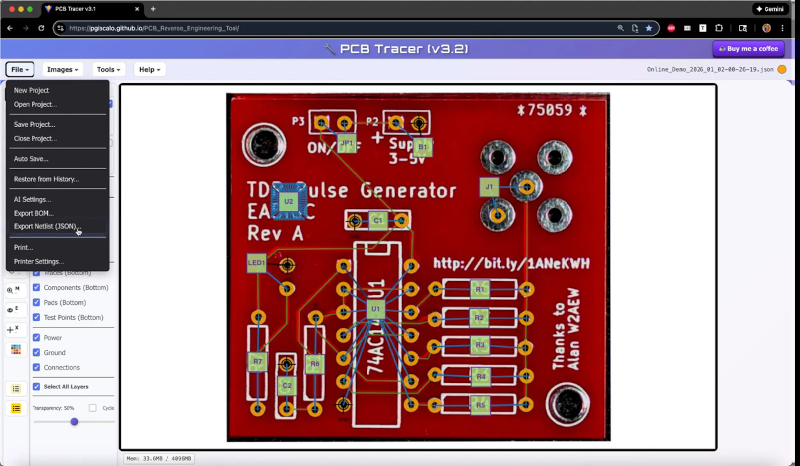
If you want to reverse engineer a PC board, you could do worse than X-ray it. But thanks to [Philip Giacalone], you could just take a photo, load it into PCB Tracer, and annotate the images. You can see a few of a series of videos about the system below.
The tracer runs in your browser. It can let you mark traces, vias, components, and pads. You can annotate everything as you document it, and it can even call an AI model to help generate a schematic from the net list.
This is one of those things that you could do without. Any photo editor could do the same thing. But having the tool aware of what the photo is showing makes life easier. The built-in features are free, but if you use the AI tool, he says it will cost you about a half-dollar per schematic (paid to the AI company).
Even if you don’t think you need to reverse-engineer anything, you may still find this useful if you are trying to understand a board for repair. We’ve had a good Supercon/Remoticon talk about PCB reverse engineering you can watch. If you want to see what a real X-ray of a board looks like, here you go.


Or just send it to Big Clive.
One moment please…
This document gives an overview of the many features of PCB Tracer. It is much more than a drawing program and is very data-rich. The software creates, reads and writes a number of different file types. These include netlists, schematics, pdf datasheets, project files, project history, BOM, and PCB photos. https://pcbtracer.com/PCB_Tracer.html
“The tracer runs in your browser.”
No. It runs in some browsers. Apparently not the one I use. If a site is explicitly made on purpose to not work in whatever browser I open it with, that site gets blocked and never again will I have to see their content.
Is w3m giving you troubles again?
Same for me with Firefox on Linux. Anyway, it’s visibly made for the botnet by Google (TM). I don’t participate to this botnet.
As much as I don’t want to switch away from Firefox, every time I hit yet another webapp that can’t run because FF’s management refuse to implement the standards I get one step closer…
(they claim it’s for “safety” but they’d rather force you to use a native app instead with zero sandboxing. That’s not promoting user safety, that’s just avoiding responsibility.)
Remember when the browser was going to be the universal OS or something?
I had a short peek at: https://pcbtracer.com/
And the first (only) thing I see is: “Browser Not Supported. PCB Tracer requires a browser that supports access to a local directory.”
Ah yes. I am not going to give a web browser access to my whole file system. I really avoid smoking the stuff that makes people want to do things like that.
Safety comes in layers. This brings up memories of the complete madness of “autorun” CD’s in the way Microsoft likes it, combined with the Sony rootkit on audio CD’s that wreaks all kind of havoc on your PC. Do you still remember that? Microsoft has always neglected safety whenever some perceived “convenience” could be achieved. And then they leave the mess they create to people creating anti-virus software.
It’s one of the reasons I switched to Linux over 10 years ago. Linux also has it’s problems, but at least there is very little malice in it, and when some is found it’s quickly fixed and the holes are plugged.
I’ve never had a virus on my PC. I neither need microsoft, nor anti virus software. But then again, I don’t run dubious software from unknown sources either.
As the developer, I totally understand concerns about browser compatibility and about file permissions. With that in mind, a desktop version is currently under active development. It’ll have a lot more features, including support for any number of PCB layers, support for surface mounted ICs and additional AI intelligence features.
As long as the AI features can be turned off.
Better sand down the PCB and reverse-engineer it in KiCad.
https://hackaday.com/2024/04/23/reverse-engineering-the-quansheng-hardware/
or just burn it completely, and you´ll have all the traces and dies exposed.
ha. im in the middle of this process to reverse engineer a soviet era wire recorder. two sided pcb with ancient looking parts. i took a picture of the front an loaded it in inkscape. there i made three layers: one for the parts, and one each for the sides. using the line tool i draw the connections. i use my own untelligence to convert that to a schematic. manual labor indeed. i count it as a learning experience
I am trying to like this. I like the goal of the tool, and he clearly put quite some thought and effort into this.
But I’m having difficulty in comprehending the benefits of this, compared to just using KiCad.
In KiCad, you can also import background images and draw over them. Both with real footprints from KiCad’s library, and with copper tracks. One of the main questions is: What do you have when you’ve done the hard work? In KiCad, you’ve got a fully reverse engineered PCB, and you can easily create Gerbers from it, or add the schematic. With this tools, I’m not sure what you can do after the PCB has been drawn over. Are there any export functions, or are those not finished yet?
@51:00 he mentioned an export of the netlist to KiCad, and for hints of how that might work. But this is not how it works at the moment in KiCad. In KiCad a full reverse engineer workflow is sort of:
Make pictures of the PCB. Picture quality matters. From depopulating the PCB, to sanding off the PCB to expose inner layers (It has all been done and also documented sometimes)
Do a rough import of the pictures in the PCB editor. Place some footprints on top to get a few references. Draw the PCB outline according to real dimensions. The pictures can be scaled and rotated in KiCad if that’s needed.
Export the footprints into a program that is good with working with pictures (Gimp, Krita, etc).
Also import the photographs into this graphics program (This is beyond KiCad).
You can use export from KiCad as a guideline to reduce distortions from the photographs.
Use the graphics program to enhance contrast of the photographs.
Import the improved pictures back into KiCad.
Build up more of the PCB. Place footprints, retrace the tracks.
Assign net names.
Or slightly better: First draw the symbols in the schematic, assign footprints, and “Update PCB from Schematic [F8]” to get the footprints on the PCB. If you do it in this order, there is already a connection between symbols and footprints.
Draw tracks. Drawing tracks in between footprints on the PCB is still a bit fiddly in KiCad, but it can be done.
You can assign net names to the tracks. Having different netnames allows KiCad to keep clearances in between different nets.
You can use: “Update Schematic from PCB” (the other way around from the normal workflow) to get the netlist into the schematic. This does not draw tracks, but it does attach labels with the net names directly to pins in the schematic.
From there, the schematic can be further cleaned up and extended.
This is an iterative process. In the end the schematic and the PCB will match each other. On the schematic it’s easy to see whether all connections are “plausible”.
In the end there should be no DRC violations or missing parts after an “Update PCB from Schematic [F8]”.
At this moment you have a full working KiCad project. Use it as a start to make a variant of the project, or create Gerbers and order PCB’s.
There are (probably) a few things this PCB Tracer program can do better then KiCad, but how much is it lacking by having to learn another program, and unknown (to me) export capabilities? Having to redo half the work all over to get it into a PCB design program also reduces the usefulness of this tool.
So overall, I want to err on the cautiousness side. I do not know enough of this program to really compare it with what can be done in KiCad. (I spend about 15 minutes on the 51 minute video to see some highlights) But I do wonder whether the creator of this tool is aware of the reverse engineering functionality that is slowly being built into KiCad?
Excellent comments, thanks.
I’m the creator of PCB Tracer. It started out as a little project purely for fun and learning. It remains a very fun to develop and the AI integration has some features that I think are kinda innovative. Anyway, the s/w reached a point in development where I figured I’d make it available –for free– hoping some others might finds it useful. I’ve had some very nice feedback and some complaints. I suppose that’s just the nature of going public with any project. Oh, well…
Development will continue and a desktop version is coming that will have more capabilities (support for any number of PCB layers, surface mounted component support, and more AI features). KiCad file support remains a high priority goal. But I’ll need to reverse engineer kicad file schema(s) first, since they aren’t published anyplace that I’ve seen.
Kicad PCB file is just ascii LISP file
https://dev-docs.kicad.org/en/file-formats/sexpr-pcb/index.html
(kicad_pcb
(version 20241030)
(generator “pcbnew”)
(generator_version “8.99”)
PCB Tracer now generates KiCad schematic files. In addition, it has new analysis features that produce pdf reports explaining what the circuit does and how it works.
Hi all,
I’m the developer of PCB Tracer. It’s a project I started just for fun, exploration and learning. After a few months of coding, it had enough capabilities and conveniences that I figured I’d make it freely available, hoping some people might find it useful. I’ve had enough positive feedback that I think it does have some unique abilities and some are finding it useful.
As for some of the comments here, I completely understand the frustrations about browser incompatibilities and about requests for KiCad schematics. I am working on a desktop version that will eliminate the browser concerns. The desktop version will also have more advanced features, such as support for any number of layers, surface mounted components/BGAs, additional AI features, and more.
As for KiCad schematics, I have tried several times and failed to get KiCad schematic generation working. On my TODO list is reverse engineering KiCad file schema(s). I’ve been unable to find them anywhere and think I need a better understanding of the file structures to get KiCad schematics working.
Use of PCB Tracer exploded after this story was posted. Many thanks to Al Williams for the post.
I hope some folks on hackaday will find the tool useful. If you have suggestions or questions, please send me feedback via the Help menu. When asked for new features, I typically add them within 3 days.
Thanks everyone,
Phil
A quick google:
https://dev-docs.kicad.org/en/file-formats/sexpr-schematic/index.html
https://dev-docs.kicad.org/en/file-formats/sexpr-pcb/index.html
And of course it is fully self documented https://gitlab.com/kicad/
Good job and put on your resume (seriously). But society does not need another web tool “–for free–”, put your effort in extending KiCad – it is free and open source. But if you are trying to bootstrap a business it really is meh from the ROI point of view.
Thanks. I’m just a geek having fun in retirement building stuff with technology. Keeps the mind busy and happy. Seems in the spirit of hackaday.
I’m just testing this tool by reverse engineering a power supply.
I’m finding it very useful and easy to use. The video tutorial explains all the features, so it is easy to get going.
I quite like the tools for manipulating and aligning the PCB pictures. Adding traces, vias and components is rather simple and intuitive. All in all, a very useful tool to reverse engineer a circuit with little time investment.
And I am no browser fundamentalist. I do have my favorite browser, and also a few less favorite ones, of course. But I have no quibbles on using one or another when there is an advantage, and using this tool is reason enough for using e.g. Chrome, even if I don’t use it for much else.
Thanks very much, Mr Giacalone!
Thank you for your very nice comment. PCB Tracer has a growing community of users around the world.
The AI features don’t do anything, unless you opt in.