[Hans Summers] runs a site qrp-labs.com, selling self-assembly kits mostly for radio gear and GPS applications, and had some production problems with his QCX-mini QRP transceiver kit. They were using an assembly house that had some problems with a sub-contractor going under during the pandemic, and the replacement service was somewhat below the expected level of quality, resulting in a significant number of SMT populated boards coming out non-functional. Obviously, not wanting to pass these on to customers as a debug problem, they set to work on an in-house QA test jig, to give them the confidence to ship kits again. The resulting functional test jig, (video, embedded below) takes a fairly interesting approach. Skip the video to 9:00 for the description of the test jig and detailed test descriptions.
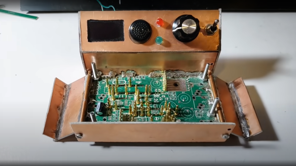
By taking an existing known-good PCB, stripping off all the SMT parts, and moving the through hole components to the rear PCB side, pogo pins could be soldered to strategic locations. Building the assembly into a rudimentary enclosure made from sawn-up raw copper clad board, with the pogos facing upwards, and a simple clamp on top, allowed the PCB-under-test (let’s call it the UUT from hereon) to be located and clamped in place. This compressed the pogos in order to make a firm electrical contact. A piece of MDF that had been attacked with a dremel did duty as a pressure plate, with cutouts around the SMT component areas to achieve the required uniform board pressure and keeping the force away from the delicate soldered parts. All this means that with an UUT connected via pogo pins to a through-hole only test PCB, the full circuit would be completed, if and only if the UUT was completely functional, and that means defect-free soldering and defect-free components.
Next the firmware was rewritten to do duty as the test controller, which when powered up would step through a sequence of test scenarios and measurements, logging the results to an OLED display and a serial interface. This rig survived 1,000 SMT tests without failing, giving [Hans] the confidence to ship out new kits and providing a database of datalog results as a backup should a customer have an issue during final assembly. All-in-all a smart idea to solve a difficult problem, with nary a custom test jig PCB in sight!
These pages have been graced with many a pogo-based test rig over the years. Here’s one to start, and if you’ve got a handy laser cutter and some scrap wood, making an accurate test rig is no bother either.
Continue reading “Production PCB And Pogo Pins Produce A Clever Test Jig” →