[xsdb] had a real problem. His JBL L8400P 600 watt subwoofer went up in flames – literally. Four of the large capacitors on the board had bulged and leaked. The electrolyte then caused a short in the mains AC section of the board, resulting in a flare up. Thankfully the flames were contained to the amplifier board. [xsdb’s] house, possessions, and subwoofer enclosure were all safe. The amplifier board however, had seen better days. Most of us would have cut our losses and bought a new setup. Not [xsdb] he took on the most extreme PCB repair we’ve seen in a long time.
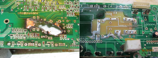
After removing the offending caps and a few other components, [xsdb] got a good look at the damage. the PCB was burned through. Charred PCB is conductive, so anything black had to be cut out. The result was a rather large hole in the middle of an otherwise serviceable board. [xsdb] had the service manual for the JBL sub. Amazingly, the manual included a board layout with traces. Some careful Photoshop work resulted in an image of the section of PCB to be repaired. [Xsdb] used this image to etch a small patch board.
The amplifier and patch were milled and sanded to match up nearly perfectly. Incredibly, all the traces aligned. [Xdsb] soldered the traces across the join with small sections of wire and solder wick. After soldering in some new high quality capacitors, the amplifier was back in action!
If you’re a big fan of burned PCB’s, check out Hackaday Prize Judge Dave Jones latest EEVblog video, where he works on a Ness home alarm panel with a similarly cooked section of FR4.
[Thanks for the link JohnS_AZ!]


