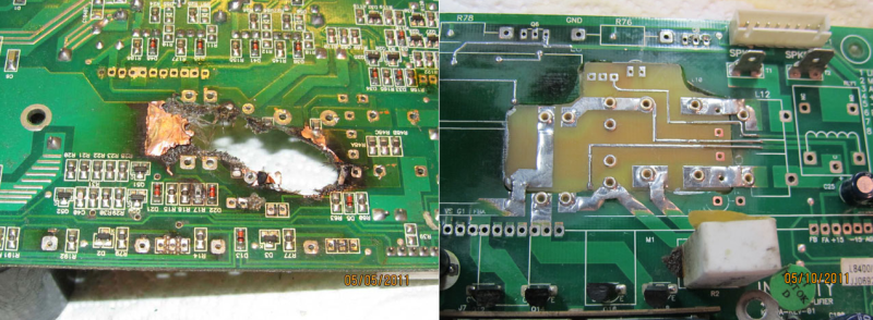
[xsdb] had a real problem. His JBL L8400P 600 watt subwoofer went up in flames – literally. Four of the large capacitors on the board had bulged and leaked. The electrolyte then caused a short in the mains AC section of the board, resulting in a flare up. Thankfully the flames were contained to the amplifier board. [xsdb’s] house, possessions, and subwoofer enclosure were all safe. The amplifier board however, had seen better days. Most of us would have cut our losses and bought a new setup. Not [xsdb] he took on the most extreme PCB repair we’ve seen in a long time.
After removing the offending caps and a few other components, [xsdb] got a good look at the damage. the PCB was burned through. Charred PCB is conductive, so anything black had to be cut out. The result was a rather large hole in the middle of an otherwise serviceable board. [xsdb] had the service manual for the JBL sub. Amazingly, the manual included a board layout with traces. Some careful Photoshop work resulted in an image of the section of PCB to be repaired. [Xsdb] used this image to etch a small patch board.
The amplifier and patch were milled and sanded to match up nearly perfectly. Incredibly, all the traces aligned. [Xdsb] soldered the traces across the join with small sections of wire and solder wick. After soldering in some new high quality capacitors, the amplifier was back in action!
If you’re a big fan of burned PCB’s, check out Hackaday Prize Judge Dave Jones latest EEVblog video, where he works on a Ness home alarm panel with a similarly cooked section of FR4.
[Thanks for the link JohnS_AZ!]


Well done, uses many ideas I’d probably have tried given time.
Kudos to the OP for some extremely innovative repairs, he should apply to the ESA :-)
On the subject of PCB repair, how about someone using a dead Bluray drive optical module with replacement BDR diode and stepper motor to make a circular PCB developer? this might actually work and would be fine for small PCBs which don’t justifying the expen$e of sending them away to be made.
Wow! I have been a daily reader of Hackaday since the beginning, but to see my own work appear here is truly an honor! Thank you all for the comments.
-XSdB
An honor? Man that PCB repair is insane. I’m from the gang that would have either given up or tried to salvage the amp board from a broken one, not repair the board like Frankenstein.
Good job!
That’s heavy!
I did have a similar issue with another JBL sub. I didn’t have the manual with schematics but the hole in the PCB was also a lot smaller.. Extreme indeed!
THIS is a hack, literally. Actually hacked out a chunk of pcb and replaced it! This is the kind of work I like to see on HAD, fixing something that most people would have sent to the trash. My compliments to the hacker.
agreed.
seconded
thirded.
C-C-C-C-C-C
Fourthed.
Kudos
farted. oops :o)
aww yiss.
sevened.
The images of your daily email newletter don’t load since you redesigned the site. I’ve reported it before, but it is still not fixed. Please fix it. Hackaday’s daily newsletter is the best thing I read every morning. Thank you.
Same goes for the individual article emails. Shame really.
This is awesome!, I’ll think twice about chucking dodgy pcbs from now on.
It should be pointed out this obviously only works since it’s a 2 layer PCB. Obviously any multilayer PCB is total junk once it burns through an inner layer. Frequently they’re junk even before that, because the heat causes the internal layers to start separating, breaking plated-through vias.
Not necessarily. I know of military personnel whose avionics training included the repair of a multi-layer board that had a hole blown through it by lightning. I sorta remember it being 7 layers, but know for certain it was more than two. Of course, being military, he had access to the specs of the circuit card so knew where all of the traces needed to be.
Granted, it was a very expensive board from a multi-multi-million dollar aircraft. In the end, it was certified for flight. He has a much, much higher tolerance for detail and tedium than I do.
Meanwhile, out in the real world . . . yeah, it’s junk.
Nope!!!,
There is a repair standard for multi layer PCBs
‘IPC-7721 Repair and Modification of Printed Boards and Electronic Assemblies’
It’s truly an electronic engineers wet dream, especially the photographs, brings a tear to my eye every time I read it.
Yep, using the IPC-7721 I do repairs in four layer boards.
And I’m just in the train maintenance business.
But when you have old equipment, yhat’s not replaceable, you have to do repairs like these.
Regards,
Lerche
I salute thee King of all Hackers!
I usually say that if there’s still a pcb with holes, it can be fixed….. this is proof to the contrary, but I dont think I’ll let on…. good work!
There was still PCB with holes – it just had one big hole too much. :-)
Intarsia!
A bit risky to keep those 15000uF Caps still in there after such a blast. They might be the next that will fail.
he chucked the electrolytic caps that caused the problem in the first place, and replaced them with much more expensive poly caps.
Are youn sure? The caps in the picture with the fried board do look like the ones in the last images. You know that we talk about the black 15000uF caps on the right and not the one that are exploded into pieces, right?
“The inferior electrolytic bipolar caps were replaced with polypropylene which will NEVER fail again!”
This amp has been operating in daily use for over 5 years after that repair. I’m quite sure. ;)
-Make that 4 years :)
Where’s the Arduino? It’s not a hack without it..
seconded
This is my favourite article on HaD in a long time
respect!
Funnily, I had a similar problem just a few days ago.
The pcb of an old amp (from somewhen in the 80s) had a bad transistor, there was a lot of heat. It did not go up in flames, but still a lot of damage.
I poured some epoxy into the hole after covering one side with tape. Worked perfectly well, although [xsdb]’s solution is way more classy :)
Great stuff.
Shows the benefit too of having the service materials available and not treated as some kind of trade secret as they are by a lot of companies.
That’s astounding work, xsdb. Really well done, and especially nice work on lining up all the layers from the diagrams and the actual circuit board.
Bondo works for pretty good for PCB repair ( yes, the stuff you fix a fender dent with)
Absolutely fabulous job. I have spent a lot of time dealing with dead Strand Lighting dimmer circuits that tended to burn out. If I could manage a repair that beautiful I would be a happy man.
That is some nice repair and rework, [xsdb]! Don’t think I’ve ever seen it done quite that way, or that well.
Kudos to JBL for including for including a board/trace layout, also.
The photos of the freshly grafted bit of PCB, prior to any soldering, are my favorite. Man, that is some serious gonzo repair work. :D
Multilayer boards are repairable, see the folks doing Iphone 5 repairs who use nano sized wire to repair damage caused by using the wrong length screws.
I’ve heard of X-rays being used to find the one O/C trace and reroute around it, often this works.
Another trick not often used is an impedance scan to adjacent traces, the traces either side of a break will also show a different impedance to ground than control traces.
Works for me anyway.
Always the question how valuable the board is. The screw story is one more reason for me to avoid electronics with the logo of the rotting (bitten) apple at all cost.
Now this is next level board repair, and i thought i was extreme! LOVE IT!