If you’ve ordered PCBs from Seeed Studio, ITead, DirtyPCB, or another board house in China, you’ve probably noticed that neat little 100% e-test option available on the order form. If you select this, the board house will throw your PCBs in a machine that will poke a pin in every pad to make sure all the connections are good. Less work for you, right? As [Andy] found out, not always. He was bitten by a manufacturing defect that sheds some light on what that e-test actually is, and the capabilities of what these Chinese board houses can do.
Most of [Andy]’s project have a lot of surface mount components, and when he receives his boards, he notices a few pin pricks on each and every pad. This is from a flying lead machine; a robotic continuity checker that makes sure all the relevant pads are electrically isolated from each other.
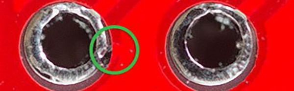
One of [Andy]’s recent projects is an entirely through-hole design. Apparently these robotic meters don’t test through-hole pads; it’s significantly harder to measure the continuity of a hole rather than a pad, apparently. After assembling one of these boards, he noticed a problem where one of the GPIOs was permanently high. The offending trace was found underneath a DIP socket, in precisely the worst possible place it could be.
If [Andy] had inspected the board beforehand, this problem would have been avoided. He says it was a relatively simple board with big traces and wide spaces and he didn’t think a manufacturing defect was possible. He was wrong, and now we have a warning. We thank him for that.


