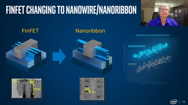
Intel’s CTO says the company will eventually abandon CMOS technology that has been a staple of IC fabrication for decades. The replacement? Nanowire and nanoribbon structures. In traditional IC fabrication, FETs form by doping a portion of the silicon die and then depositing a gate structure on top of an insulating layer parallel to the surface of the die. FinFET structures started appearing about a decade ago, in which the transistor channel rises above the die surface and the gate wraps around these raised “fins.” These transistors are faster and have a higher current capacity than comparable CMOS devices.
However, the pressure of producing more and more sophisticated ICs will drive the move away from even the FinFET. By creating the channel in multiple flat sheets or multiple wires the gate can surround the channel on all sides leading to even better performance. It also allows finer tuning of the transistor characteristics.
Continue reading “Intel Says Nanowire And NanoRibbon In Volume In Five Years”


