Intel Says Nanowire And NanoRibbon In Volume In Five Years

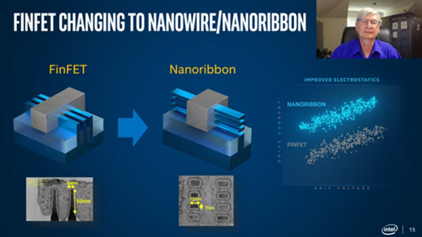
Intel’s CTO says the company will eventually abandon CMOS technology that has been a staple of IC fabrication for decades. The replacement? Nanowire and nanoribbon structures. In traditional IC fabrication, FETs form by doping a portion of the silicon die and then depositing a gate structure on top of an insulating layer parallel to the surface of the die. FinFET structures started appearing about a decade ago, in which the transistor channel rises above the die surface and the gate wraps around these raised “fins.” These transistors are faster and have a higher current capacity than comparable CMOS devices.

However, the pressure of producing more and more sophisticated ICs will drive the move away from even the FinFET. By creating the channel in multiple flat sheets or multiple wires the gate can surround the channel on all sides leading to even better performance. It also allows finer tuning of the transistor characteristics.

Continue reading “Intel Says Nanowire And NanoRibbon In Volume In Five Years”

Silicon Nanowires Create Flexible Photodetectors

Modern display and solar cell technologies are built with a material called Indium Tin Oxide (ITO). ITO has excellent optical transparency and electrical conductivity, and the material properties needed for integration in large-scale manufacturing. However, we’re not content with just merely “good enough” nowadays, and need better materials to build ever better devices. Graphene and carbon nanotubes have been considered as suitable replacements, but new research has identified a different possibility: nanowires.

Researchers from the Indian Association for the Cultivation of Science (IACS) and the Centre for Research on Adaptive Nanostructures and Nanodevices (CRANN) in Ireland have demonstrated a seamless silicon nanowire junction that can be used for photodetector and display technology.

Before you get lost in the jargon, let’s take a step back. A nanowire is just a very narrow length of wire, on the order of 1 nanometer across. When silicon is used at this scale, electrical charges can become stuck (called “charge trapping”), which means that the holes and electrons are separated, allowing for transistors and photovoltaics. By controlling where these holes form in the nanowire, you can create a “seamless” junction without using any dopant materials to create impurities, as is done in modern CMOS transistors

These material properties allow the functionality of a junction, but it still needs to be easily and repeatably manufactured. To solve this problem, the team put the nanowire transistors on a flexible polymer, which should enable flexible nanowire applications, such as a roll-up screen.

The first step towards a display is a simple photodetector, just consisting of a basic P-N junction, but they hope this technology will eventually be useful in “smart windows” due to the junctions’ applicability to photodetectors and cameras. Moving to emitting light for displays or creating a solar cell using this technology will probably take some time.

Do you have any experience with different materials for creating junctions? What would you do with a small, transparent photodetector? We’ve featured homebrew solar cells before, as well as creating DIY semiconductors. We’ve also seen silver nanowires for wearable circuits.

[Via IEEE Spectrum]

Print, Rinse, Wear. Nanowire Circuits For Your Microfibre Clothing.

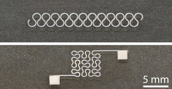
While our bodies are pretty amazing, their dynamic nature makes integrating circuits into our clothing a frustrating process.  Squaring up against this challenge, a team of researchers from North Carolina State University have hit upon a potential boon for wearable electronics: silver nanowires capable of being printed on flexible, stretchy substrates.

It helps that the properties of silver nanowires lend themselves to the needs of wearable circuits — flexible and springy in their own right — but are not without complications. Silver nanowires tend to clog print nozzles during printing, so the research team enlarged the nozzle and suspended the nanowires in a water-soluble solvent, dramatically cutting the chance of clogging. Normally this would have a negative impact on precision, but the team employed electrostatic force to draw the ink to the desired location and maintain print resolution. Once printed, the solvent is rinsed away and the wearable circuit is ready for use.

By controlling print parameters — such as ink viscosity and concentration — the team are able to print on a wide variety of materials. Successful prototypes thus far include a glove with an integrated heating circuit and an electrocardiograph electrode, but otherwise the size of the printer is the only factor limiting the scale of the print. Until this technique becomes more widely available, interested parties might have to put their stock into more homebrew methods.

[Thanks for the tip, Qes!]

Nanowire Batteries Never Need Replacing

In this day and age we’re consistently surrounded with portable electronic devices. In order for them to be called “portable”, they must run on batteries. Most, if not all, use rechargeable batteries. These batteries have a finite lifespan, and will eventually need to be replaced. UCI chemist [Reginald Penner] and doctoral candidate [Mya Le Thai] have been hard at work on making rechargeable batteries that last forever.

Nanowires are great candidates for rechargeable battery technology because the wires, thousands of times thinner than a human hair, are great conductors of electricity. The problem is repeated charging and discharging makes them brittle, which causes them to eventually fail. Typically, the researchers at UCI could get 5000 to 7000 cycles in before they failed. After some trial and error, they found that if they coat a gold nanowire with an acrylic-like gel, they can get up to 200,000 charge/discharge cycles through it before failure.

We’ve seen rechargeable battery hacks before, but making a battery that never needs replacing is sure to get everyone excited.