 Paper as a substrate for electronic circuits is not very common, but promising for flexible circuits with low cost and easy recyclability. That said, paper is not an easy material to work with when printing traces, as the cellulose material is both absorbent and irregular, limiting the resolution and accuracy of so-called papertronics. Even when using higher-quality paper with wax-based masks this resulted in poor resolution issues, so [Zahra Rafiee] et al. opted to approach the problem from the other direction, by using hydrophobic parchment paper as the base combined with a laser.
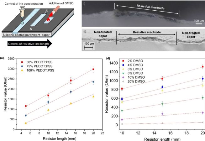
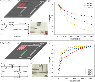
The nice thing about the inks used with papertronics that they aren’t just traces, but can also be functional elements like resistors, which is also demonstrated in the paper. The channels for the inks are created using a 50 Watt CO2 laser, which etches away the silicone coating on the parchment paper. The achieved resolution in the article is around 250 µm for line widths and 300 µm line spacing, which is much better than that for wax-based alternatives.
Continue reading “High-Density Parchment Paper Papertronics With Laser-Carved Hydrophilic Channels”