
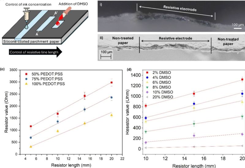
 Paper as a substrate for electronic circuits is not very common, but promising for flexible circuits with low cost and easy recyclability. That said, paper is not an easy material to work with when printing traces, as the cellulose material is both absorbent and irregular, limiting the resolution and accuracy of so-called papertronics. Even when using higher-quality paper with wax-based masks this resulted in poor resolution issues, so [Zahra Rafiee] et al. opted to approach the problem from the other direction, by using hydrophobic parchment paper as the base combined with a laser.
The nice thing about the inks used with papertronics that they aren’t just traces, but can also be functional elements like resistors, which is also demonstrated in the paper. The channels for the inks are created using a 50 Watt CO2 laser, which etches away the silicone coating on the parchment paper. The achieved resolution in the article is around 250 µm for line widths and 300 µm line spacing, which is much better than that for wax-based alternatives.
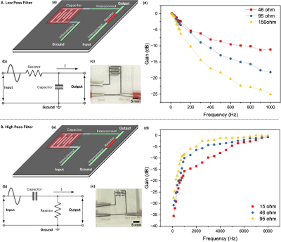
Providing conductivity in the inks was PEDOT:PSS, which, when mixed with dimethyl sulfoxide (DMSO), creates resistors. Capacitors can be printed by creating interlocking PEDOT:PSS ‘fingers’, with a Poly Vinyl Alcohol (PVA) based gel overlaid as electrolyte. These combinations were used to create RC low- and high-pass filters.
The degradation of these papertronic circuits was also tested, with them buried in soil under typical conditions. Only the silicone coating was rather immune to degradation. Since silicone is considered chemically and biologically inert, it’s claimed to not be an issue. For situations where such easy decomposition is not desirable, encapsulation with polydimethylsiloxane (PDMS) is offered as an option.









Use a “waser” water cutter for flash papertronics? ;)
I remember when painting circuits on Priority labels with conductive paint was the cool thing to do.
I remember the book “Diamond Age”, by Neal Stephenson – in the spirit of Gibson – talking about “e-ink” displays…. then suddenly we had e-ink displays. It also mentioned 3D printers; but not just for plastic – they used all kinds of elemental ingredients to be a true “replicator” technology; a civilization on the cusp of post-scarcity.
Good book.
Published in 1995, e-ink displays or “smart paper” had already existed in concepts and prototypes since the 1970’s. It only took about 15-20 years more for the talk to “suddenly” turn into useful products you could actually buy.
Most revolutionary ideas need a 50 year run-up.
I’m all for experiments with new materials; and(as we have seen in other contexts like those carbon film applications used in a lot of membrane keypads) being able to include at least some passives in the PCB can be quite handy; but I’m a little curious if we are still meaningfully talking ‘paper’ when it’s the silicone coating that we are interacting with and which is apparently critical to the exercise.
By that standard are the old ‘phenolic paper’ brown boards you typically see in fairly old or particularly undemanding circuit boards actually ‘papertronics’? It’s the phenolic resin doing much of the work; but authentic wood or cotton cellulose fiber fill in the composite material.
the silicone or wax coating is just a form of masking, like the deposition equivalent of etching’s etch-resist. the substrate is the paper itself. if i understand correctly, the circuits are formed by material that absorbs into (or surface-coats?) the paper. it’s like how we consider PCBs to be FR4 (fiberglass) rather than identifying it with the solder mask.