It’s amazing how affordable PCB fabrication has become. It has long been economical (although not always simple) to fabricate your own singe and double-sided boards at home, the access to professional fabrication is becoming universal. The drive continues downward for both cost and turnaround time. But there is growing interest in the non-traditional.
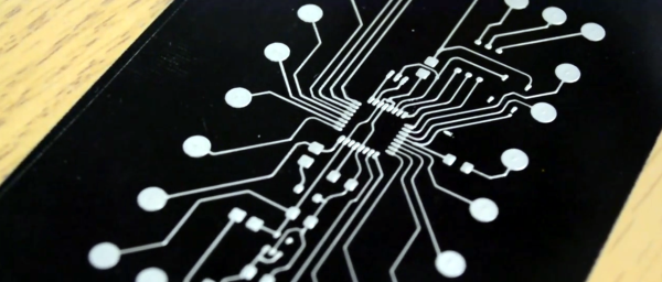
Over the last year we’ve seen a huge push for conductive-ink-based PCB techniques. These target small-run prototyping and utilize metals (usually silver) suspended in fluid (think glue) to draw traces rather than etching the traces out of a single thin layer of copper. Our question: do you think conductive in will become a viable prototyping option?
Voltera V-One Circuit Board Prototyping Machine
I recorded this interview at 2015 CES but was asked not to publish it until their crowd funding campaign went live. If you haven’t been paying attention, Voltera is at almost 400% of their $70k goal with 26 days remaining. This printer definitely works. You can print circuits, solder components or reflow them, and there’s even a second non-conductive ink that can be used to insulate between traces when they cross over one another. In the video [Alroy] suggests Voltera for small production runs of 10-20 boards. Would you see yourself using this for 10-20 boards?
Personally, I think I could solder point-to-point prototypes in less time. Consider this: the V-One will print your traces but you still must solder on the components yourself. If the board design reaches a high level of complexity, that timing may change, but how does the increased resistance of the ink compared to copper traces affect the viability of a board? I assume that something too complex to solder point-to-point would be delving into high-frequency communications (think parallel bus for LCD displays, etc.). Is my assumption correct? Do you think conductive ink will get to the point that this is both viable and desirable over etching your own prototypes and how long before we get there?
Now, I certainly do see some perfect use-cases for Voltera. For instance, introduction to circuit design classes. If you had one of these printers at the middle school or high school level it would jump-start interest in electronics engineering. Without the need for keeping chemical baths like Cuperic Chloride or Ferric Chloride on hand, you could walk students through simple board design and population, with the final product to take home with them. That’s a vision I can definitely get behind and one that I think will unlock the next generation of hardware hackers.
Correction: [Arachnidster] pointed out in the comments that Voltera is still working on being able to reflow boards printed by the V-One. On their Kickstarter page they mention: “(Reflow onto Voltera printed boards is currently under development)”


