Physics-Controlled Component Auto-Placer

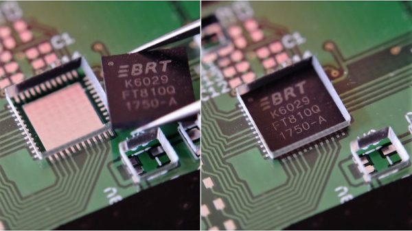
[Jarrett] recently stumbled upon a class of drawing algorithms called force-directed graphs, which artificially apply forces to the elements. The final graph is then generated by applying the laws of physics and letting the system reach equilibrium. This can often result in a pleasing presentation of things like mind maps and other diagrams without having to hand-place everything. He realized that this approach almost mimics the way he places components when doing a PCB layout. Out of curiosity or intense boredom, we’re not sure which, he decided to implement this in a tool that interacts with KiCad ( see animated GIF below the break ).

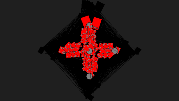
He has to ignore certain nets such as power and ground rails, because they distort the result. This simulation treats the nets as springs, and the center of each footprint behaves a charged particle. [Jarrett] added a twist, literally, to the usual implementations — each net pulls on its pin, not the part center, and therefore the chips will both rotate and be pushed around as the system stabilizes.

The results are sometimes quite striking. Useful? Dubious, but maybe!

The project code is up on GitHub, but is very experimental and he is unlikely to carry it further. Among the missing features, the Python code must be tweaked for each different netlist files and other parameters, and there is no way to feed the result back into KiCad. But this is enough for [Jarrett], who only set out to see if the concept was possible. The code is available if anyone wants to try their hand at taking this to the next level.

Continue reading “Physics-Controlled Component Auto-Placer”

Acrylic Stencils Help With Component Placement For SMD Assembly

Surface mount is where the action is in the world of DIY PCBs, and deservedly so. SMDs are so much smaller than through-hole components, and fewer holes to drill make surface-mount PCBs easier to manufacture. Reflow soldering is even a snap now thanks to DIY ovens and solder stencils you can get when you order your boards.

So what’s the point of adding another stencil to the surface-mount process? These component placement stencils are [James Bowman]’s solution for speeding up assembly of boards in production runs too small to justify a pick and place robot. [James] finds that placing small components like discrete resistors and caps easy, but struggles with the placement of the larger components, like QFN packaged microcontrollers. Getting such packages lined up exactly is hard when the leads are underneath, and he found repositioning led to smeared solder paste. His acrylic stencils, which are laser-cut from SVGs derived directly from the Eagle files with a script he provides, sandwich the prepped board and let him just drop the big packages into their holes. The acrylic pops off after placement, leaving the components stuck to the solder paste and ready for their trip to the Easy Bake.

[James] claims it really speeds up hand placement in his biggish runs, and it’s a whole lot cheaper than a dedicated robot. But as slick as we think this idea is, a DIY pick and place is still really sweet.