The vast majority of semiconductors products we use every day are primarily constructed on a silicon process, using wafers of pure silicon. But whilst the economics are known, and processes mature, there are still some weaknesses. Especially for power applications. gallium nitride (GaN) and silicon carbide (SiC) are materials that have seen an explosion in uses in the power space, driven especially by an increase in electric vehicle sales and other high-power/high-voltage systems such as solar arrays. But, SiC is expensive and very energy intensive. It looks like diamond substrates could become much more common if the work by Diamfab takes off.
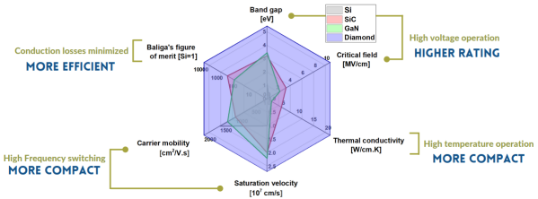
Diamond, specifically thin films of synthetic diamond formed on a suitable substrate, exhibits many desirable properties, such as a vastly superior maximum electric field compared with silicon, and a thermal conductivity five times better than copper. Such properties give diamond structures a big power and voltage advantage over SiC, which is in turn a lot better the pure silicon. This also means that diamond-based transistors are more energy efficient, making them smaller and cheaper, as well as better performing. Without the high formation temperatures needed for SiC, diamond could well be their downfall, especially once you factor in the reduced environmental impact. There is even some talk about solid-state, high-voltage diamond insulator capacitors becoming possible. It certainly is an interesting time to be alive!
We do cover news about future semiconductors from time to time, like this piece about cubic boron arsenide. We’ve also seen diamond being used as a battery, albeit a very weak radiative one.
[via EETimes]


