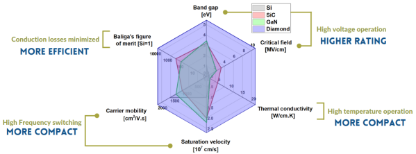
We don’t know how you feel when designing hardware, but we get uncomfortable at the extremes. High voltage or current, low noise figures, or extreme frequencies make us nervous. [Orion Serup] from CrabLabs has been turning up a few of those variables and has created a fairly beefy 3-phase motor driver using GaN technology that can operate up to 80V at 70A. GaN semiconductors are a newer technology that enables greater power handling in smaller packages than seems possible, thanks to high electron mobility and thermal conductivity in the material compared to silicon.
The KiCAD schematic shows a typical high-power driver configuration, broken down into a gate pre-driver, the driver itself, and the following current and voltage sense sub-circuits. As is typical with high-power drivers, these operate in a half-bridge configuration with identical N-channel GaN transistors (specifically part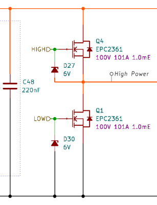 EPC2361) driven by dedicated gate drivers (that’s the pre-driver bit) to feed enough current into the device to enable it to switch quickly and reliably.
The design uses the LM1025 low-side driver chip for this task, as you’d be hard-pushed to drive a GaN transistor with discrete components! You may be surprised that the half-bridge driver uses a pair of N-channel devices, not a symmetric P and N arrangement, as you might use to drive a low-power DC motor. This is simply because, at these power levels, P-channel devices are a rarity.
Why are P-channel devices rare? N-channel devices utilise electrons as the majority charge carrier, but P-channel devices utilise holes, and the mobility of holes in GaN is very low compared to that of electrons, resulting in much worse ON-resistance in a P-channel and, as a consequence, limited performance. That’s why you rarely see P-channel devices in a circuit like this.