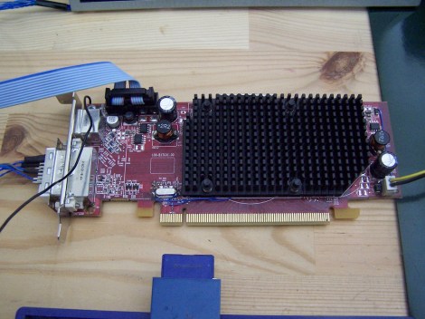
[Gpuhackr] chose his username to explain exactly how he spends his time. For instance, here he’s using an STM32 Discovery board to drive an AMD Radeon HD 2400 graphics card. The ARM microcontroller isn’t actually using the PCIe interface on the card. Instead, [Gpuhackr] has patched into the debugging interface built into the card itself. This isn’t quite as straight forward as it sounds, but if you do the wiring carefully it’s a pretty intersting way to connect an ARM to an LCD monitor.
This project would be almost impossible if it weren’t for the open source code which AMD has released. This lets him implement the card’s 3D rendering features. The demo directly programs the UVD Xtensa CPU which is on the video card. It draws a cube with color gradients on each side. The cube spins while the debug information is overlaid on the screen. In this case the ARM chip/board is really being used as a programmer to upload some custom firmware. But we think a real code-ninja could implement a communications protocol to open up a simple way to drive the card in real-time.
[Thanks uMinded]


can you say clusters..??
So… no source code, nothing at all, just a one post guy telling a story?
There was some source code at
https://github.com/gpuhackr
last year november
http://webcache.googleusercontent.com/search?q=cache:7tew3NmU2RwJ:https://github.com/gpuhackr+&cd=1&hl=en&ct=clnk&client=opera
video or it never happend
so… now my aurduino can have opencl and opengl?
so… now my aurduino can have opencl and opengl?
I2C runs at 150KB/s, so no video :(
It would be mind blowing if someone could find a way to use stand alone ATI card as a h.264 decoder, just pumping raw mpeg files with a microcontroller from SD card.
You can switch the I²C bus to be master. So you run your logic on the Tensilica CPU and use a microcontroller via I2C to give you I/O, interface to mass storage for textures, etc. It would be a bit slow yes, but choose a card with a lot of SDRAM, store the textures compressed and decompress them on the card. Any 8-bit micro with a master/slave I2C port would be sufficient.
I wonder why he didn’t release any source. He promised a Linux utility for locating the I2C pads on any arbitrary Radeon card as well as the cube rendering stuff for the Tensilica. This was published 10 months ago though. Perhaps AMD saw it and made him an offer he couldn’t refuse.
>Perhaps AMD saw it and made him an offer he
>couldn’t refuse.
yeah, this is too much with too little, smells like some NDA stuff
This is amazing, everything from being able to run a lvds panel directly from the dvi connector to adding a full blown gpu to a microprocessor, to doing so using just a i2c interface…
so many possible applications…
in b4 the bitcoin people…
The Bitcoin people will be moving away from GPUs pretty soon, as the new ASIC-based miners will make GPU mining unprofitable.
The LVDS part of this alleged hack is the best thing about it, IMHO.
I’m swimming in dead laptops, and if the answer to turning them into usable displays were “Use a Radeon and install a firmware” instead of “Negotiate with some weird East-Asian company on Ebay for a DVI-LVDS converter”, I’d be able to put at least part of them to use.
This is interesting from a research perspective, but has no practical use. The guy is learning about the UVD Xtensa CPU, and writing firmware for that. He most likely has no interest in making an arbitrary cpu drive the gpu. So it has nothing do to with the STM32, he’s probably just using it to bitbang the debug interface protocol. If you want a 32bit MCU with 3D HW Acceleration or video decoding, just get a dev. board that runs linux.
The problem with boards with embedded 3D renderers is the hardware is often not publicly documented e.g. PowerVR, Broadcom Videocore. At least with ATI it’s mostly open. I had no idea until now there was a general purpose CPU in there hanging on the bus.
The point I think is that because the Xtensa is in there, a video card is a fairly powerful single-board computer. You just need to have something to bitbang some code into it at boot (like you do with FPGAs) and then it’s off.
Exactly. It really is a very clever bit of work.
This is a WHOLE bucketful of holy s**t! Seriously. I can’t wait to see how this is taken advantage of.
Hey tmbinc – how ya doin’.
Anyway – does anyone know if the debug interface is documented ( the i2c ).
I’d like to know the commands ( presumably memory/read/write/execute ).
Alternatively – by any chance does the xtensa run code loaded via the bios ? Perhaps the debug protocol is in there ?.
I’d actually like to mess around with this – and the debug interface protocol is the only info I can’t seem to locate.
I guess the code is based on eg this demo, which seems quite involved. Maybe if you could dump compiled GLSL shaders from the proper drivers somehow then it could be bit easier.
I think this has great potential for projects needing video output. Maybe somebody could port some neat 4k demo to this :)
The hack to drive LVDS through DVI seems fairly interesting in itself too, first time I’ve heard of something like that.
I disagree with the opinion of this being non-useful.
GPUs have a lot of memory these days. You can certainly fit all resources (textures, but also vertex buffers, shaders and command buffers) in there. Uploading them would take a while (and I agree that SD card access from the UVD would be nice; not sure if that’s possible but my guess is that it is.)
After that, a small microcontroller – even an AVR! – could execute game logic, and only upload a few matrices to the GPU to update the player position etc, and then trigger re-execution of the command buffer in GPU memory. That should easily work over I2C in realtime.
Of course you could just run the game on the UVD but that’s probably not the point.
Amazing!
If I understand correctly, the STM32 is basically “just” bootstrapping the cards “auxiliary” CPU, which can then be used to run arbitrary code.
I’m sort of surprised the debug interface is using I2C, I would have expected a regular JTAG interface. Maybe there actually is a JTAG chain as well, as they typically include all large devices, and are often used for initial board testing.
I wonder if that CPU has access to any of the signals at the edge connector, because if it does, it might be possible to use those as a high-speed interface, to read data from an SD card, for instance, or maybe to interface with a network card or something similar.
JTAG is in the PCIe connector. Chances are if it’s been implemented at all it will only do boundary scan. After all, they have a whole CPU on die they can do hardware debug with and it’s memory mapped into the host’s address space.
Well, some spartan6 variants have a PCIe builtin, so a spartan6+videocard+stm32 would play nicely.
OpenCV on microcontrollers anyone?
“Normally it is not possible to interface a laptop LCD to a DVI port directly as the data encoding is different however as these GPUs are also used in laptop computers they may be switched into LVDS mode allowing the display to be attached directly.”
quite obvious if you think about it…, anyone has more info about this (so you can drive old laptop screens directly from a modded card)?
Great build !
Would it be possible to use this to have a VGA display connected to a RasPi ?
Does anyone have any hints to the I2C command structure for the debug interface ?
Address I can probably work out – but some hints to structure of read / write registers commands.
Someone must know.
The datasheets on the internet confirm that the i2c is used for debug – and that GPIO_4 is used to control it – but no descriptions of the protocols.
I’ve had contact from gpuhackr via email.
He states he does expect to release code soon.
And it went silent.
Btw i did some digging and gpuhacker is Allan MacKinnon, Founder and President at Pixel I/O
he registered GpuHacker.com couple of days before creating https://github.com/gpuhackr repository.
Company does :”Our products leverage the power of GPUs to bring “100x” improvements in performance and efficiency.”
Im thinking he doesnt want to share the code after all. Too bad.
Good work tracking him down. So it took him from April until December to get to the stage in the video above? I guess he must have a day job then.
Did you try shooting the guy an email? I’ve got a small selection R600 based cards turning up this weekend to give this stuff a try, but plan only to locate the i2c bus and try blasting it with bytes to see what gets ack’d.
If you look at the recent activity of that repository it looks like he had code uploaded in April.
Didnt bother mailing him. Im guessing he got an email from ATI (NDA and stuff).
gpuhackr has posted some more pictures.
http://www.flickr.com/photos/73923873@N05/sets/72157631771354007/
Awesome hackery! I love the wires poked into a spare dimm socket to get an I2C master at a suitable level. Must remember that for emergencies :-)
I see how hundreds of hours must have gone into this. Fair enough not wanting to release it until it’s done.
Did I just read he’s ported a Dreamcast emulator to the Xtensa? That’s going to put it in a whole new league of radicalness.