Industrial GPU Adapted For The Desktop

As technologies change and adapt, we’re often left with seemingly useless junk that has nowhere to go. Certainly anyone still sitting on a pile of floppy disks feels this way sometimes, but odds are anyone who owns a mining ASIC or an NFT can attest to that as well. The trillions of dollars flowing into GPU-based data centers will likely become the next victim of this trend, so if you want to capitalize on the losses of some venture capitalist you’ll want to figure out a way to get GPUs meant for a server into your desktop doing useful work.

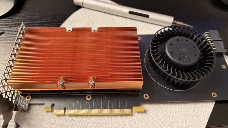
Of course, calling these devices GPUs is a bit of a stretch compared to the Radeon and GeForce cards many of us are used to using for gaming. These don’t even have a PCIe slot or video output, after all. But, as [] notes, the VRAM and GPU cores are very real and can still do useful work. An adapter board is able to mate a Tesla V100 SXM2 16 GB GPU to a standard PCIe slot, which solves the first problem, but the major downside from there is that the cooling fan for this unit was literally deafeningly loud. At 82 dB it was about as loud as a lawnmower, which is fine in a server rack but not great in a bedroom. [Oscar] found a way to tamp down the fan speed, making it usable in a home.

Without video output, the utility of these cards mainly comes from adding VRAM and compute for tasks that benefit from parallel computing. Using tensor splitting, [Oscar] is running a local LLM with this card alongside his RTX 4080, providing 32 GB of VRAM on his NixOS system. With his benchmarking tests, the LLM sports impressive stats for a self-hosted model, ranking somewhere around Claude Sonnet 4.6. What’s even more impressive is that this is all done for around £200, and with the rate the various LLM companies are ratcheting up pricing could pay itself back very quickly. If trading off performance for cost is acceptable, though, it’s possible to run local models on much less powerful hardware as well.
Getting A Proprietary-Bus GPU Onto PCIe Enables Cheaper Local LLMs, For Now

If you’ve been thinking of getting into self-hosting generative AI, but don’t have a big budget for hardware, you might want to check out [Hardware Haven]’s latest video on an unusually cheap GPU option — but you’ll have to do so quickly, before the market realizes the chance for arbitrage and prices rise accordingly.

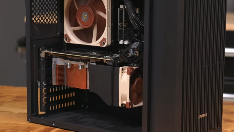
He’s gotten a hold of a 16 GB NVidia V100 card for only about a hundred bucks, mostly because it’s not easy to plug in, being on an SXM2 socket rather than the PCIe bus. SXM is a server architecture, and not something you’re likely to get on your motherboard. Another hundred got him an adapter board to fit this enterprise GPU on a consumer motherboard. That’s still a lot less than the PCIe version of the same card, which will likely set you back a thousand or more unless you get very lucky on eBay.

It’s not the newest card, dating back from 2017, but that doesn’t mean it can’t run the latest open models. After 3D printing a fan shroud for the thing so it didn’t cook itself, adding very slightly to the build cost, [Hardware Haven] set to work seeing what it could do. Going head-to-head against an RTX 3060 12 GB, the older V100 delivered more tokens per second at a  slightly higher efficiency — but much higher idle power.

Still, it’s nice to see a cheap way to get into local AI, even if it might not still be cheap by the time you read this. Once you have the hardware, you might want some easy software options so you don’t have to spend all day on setup. Of course you only need a hefty GPU to run larger models — you can get into hosting your own AI on a Raspberry Pi, if you’re patient.

Continue reading “Getting A Proprietary-Bus GPU Onto PCIe Enables Cheaper Local LLMs, For Now”

Implementing PCIe Over Fiber Using SFP Modules

Although we can already buy commercial transceiver solutions that allow us to use PCIe devices like GPUs outside of a PC, these use an encapsulating protocol like Thunderbolt rather than straight PCIe. The appeal of  [Sylvain Munaut]’s project is thus that it dodges all that and tries to use plain PCIe with off-the-shelf QSFP transceivers.

As explained in the intro, this doesn’t come without a host of compatibility issues, least of all PCIe device detection, side-channel clocking and for PCIe Gen 3 its equalization training feature that falls flat if you try to send it over an SFP link. Fortunately [Eli Billauer] had done much of the leg work already back in 2016, making Gen 2 PCIe work over SFP+.

The test setup involves a Raspberry Pi 5 on a PCIe breakout board and a PCIe card connected to the whole QSFP intermediate link with custom SFP module PCBs for muxing between PCIe edge connector or USB 3.0 connectors to use those cheap crypto miner adapter boards. The fiber is just simple single-mode fiber. Using this a Gen 2 x1 link can be created without too much fuss, demonstrating the basic principle.

Moving this up to Gen 3 will be challenging and will be featured in future videos, involving more custom PCBs. With Gen 5 now becoming standard on mainboards, it would be great to see this project work for Gen 3 – 5 at link sizes of x4 and even x16 so that it might be able to run external GPUs at full bandwidth unlike Thunderbolt.

Thanks to [zoobab] for the tip.

Continue reading “Implementing PCIe Over Fiber Using SFP Modules”

PCB Design Review: M.2 SSD Splitter

Today’s PCB design review is a board is from [Wificable]. iI’s a novel dual-SSD laptop adapter board! See, CPUs and chipsets often let you split wide PCIe links into multiple smaller width links. This board relies on a specific laptop with a specific CPU series, and a BIOS mod, to put two M.2 NVMe SSDs into a single SSD slot of a specific series’ laptop.

This board has two crucial factors – mechanical compatibility, and electrical function. Looking into mechanics, it’s a 0.8 mm thick PCB that plugs into a M.2 socket, and it has sockets for two SSDs on it – plenty of bending going on. For electronics, it has a PCIe REFCLK clock buffer, that [Wificable] found on Mouser – a must have for PCIe bifurcation, and a must-work for this board’s core! Apart from that, this is a 4-layer board, it basically has to be for diffpairs to work first-try.

Of course, the clock buffer chip is the main active component and the focus of the board, most likely mistakes will happen there – let’s look at the chip first.

Continue reading “PCB Design Review: M.2 SSD Splitter”

Cheap FPGA PCIe Development

Typically, if you want to build an FPGA project inside a PC, you’d need a fairly expensive development board that plugs into the bus. However, [CircuitValley] found some IBM RS-485 boards that are little more than a PCIe board with an Intel FPGA onboard. These are widely avaiable on the surplus market for around $20 shipped. He’s been documenting how to use them.

The FPGA onboard is a Cyclone IV with about 21,000 logic elements and a little over 750 kbits of memory. The board itself has configuration memory, power management, and a few connectors. The JTAG header is unpopulated, but the footprint is there. You simply need to supply a surface-mount pin header and an external JTAG probe, and you can program. Even if you aren’t interested in using an FPGA board, the reverse engineer steps are fun to watch.

The situation reminds us a little of the RTL-SDR — when a device uses a programmable device to perform nearly all of its functions, it is subject to your reprogramming. What would you do with a custom PCIe card? You tell us. Need a refresher on the bus? We can help. Thinking of building some sort of FPGA accelerator? Maybe try RIFFA.

Continue reading “Cheap FPGA PCIe Development”

Homebrew GPU Tackles Quake

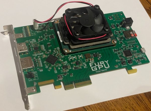
Have you ever wondered how a GPU works? Even better, have you ever wanted to make one? [Dylan] certainly did, because he made FuryGPU — a fully custom graphics card capable of playing Quake at over 30 frames per second.

As you might have guessed, FuryGPU isn’t in the same league as modern graphics card — those are made of thousands of cores specialized in math, which are then programmed with whatever shaders you want. FuryGPU is a more “traditional” GPU, it has dedicated hardware for all the functions the GPU needs to perform and doesn’t support “shader code” in the same way an AMD or NVIDIA GPU does. According to [Dylan], the hardest part of the whole thing was writing Windows drivers for it.

On his blog, [Dylan] tells us all about how he went from the obligatory [Ben Eater] breadboard CPU to playing with FPGAs to even larger FPGAs to bear the weight of this mighty GPU. While this project isn’t exactly revolutionary in the GPU world, it certainly is impressive and we impatiently wait to see what comes next.

Continue reading “Homebrew GPU Tackles Quake

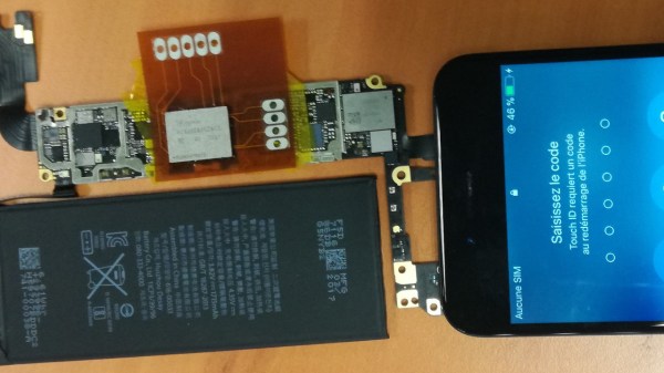
The FPC adapter shown soldered between the BGA chip and the phone's mainboard, with the phone shown to have successfully booted, displaying an unlock prompt on the screen

IPhone 6S NVMe Chip Tapped Using A Flexible PCB

Psst! Hey kid! Want to reverse-engineer some iPhones? Well, did you know that modern iPhones use PCIe, and specifically, NVMe for their storage chips? And if so, have you ever wondered about sniffing those communications? Wonder no more, as this research team shows us how they tapped them with a flexible printed circuit (FPC) BGA interposer on an iPhone 6S, the first iPhone to use NVMe-based storage.

The research was done by [Mohamed Amine Khelif], [Jordane Lorandel], and [Olivier Romain], and it shows us all the nitty-gritty of getting at the NVMe chip — provided you’re comfortable with BGA soldering and perhaps got an X-ray machine handy to check for mistakes. As research progressed, they’ve successfully removed the memory chip dealing with underfill and BGA soldering nuances, and added an 1:1 interposer FR4 board for the first test, that proved to be successful. Then, they made an FPC interposer that also taps into the signal and data pins, soldered the flash chip on top of it, successfully booted the iPhone 6S, and scoped the data lines for us to see.

This is looking like the beginnings of a fun platform for iOS or iPhone hardware reverse-engineering, and we’re waiting for further results with bated breath! This team of researchers in particular is prolific, having already been poking at things like MITM attacks on I2C and PCIe, as well as IoT device and smartphone security research. We haven’t seen any Eagle CAD files for the interposers published, but thankfully, most of the know-how is about the soldering technique, and the paper describes plenty. Want to learn more about these chips? We’ve covered a different hacker taking a stab at reusing them before. Or perhaps, would you like to know NVMe in more depth? If so, we’ve got just the article for you.

We thank [FedX] for sharing this with us on the Hackaday Discord server!